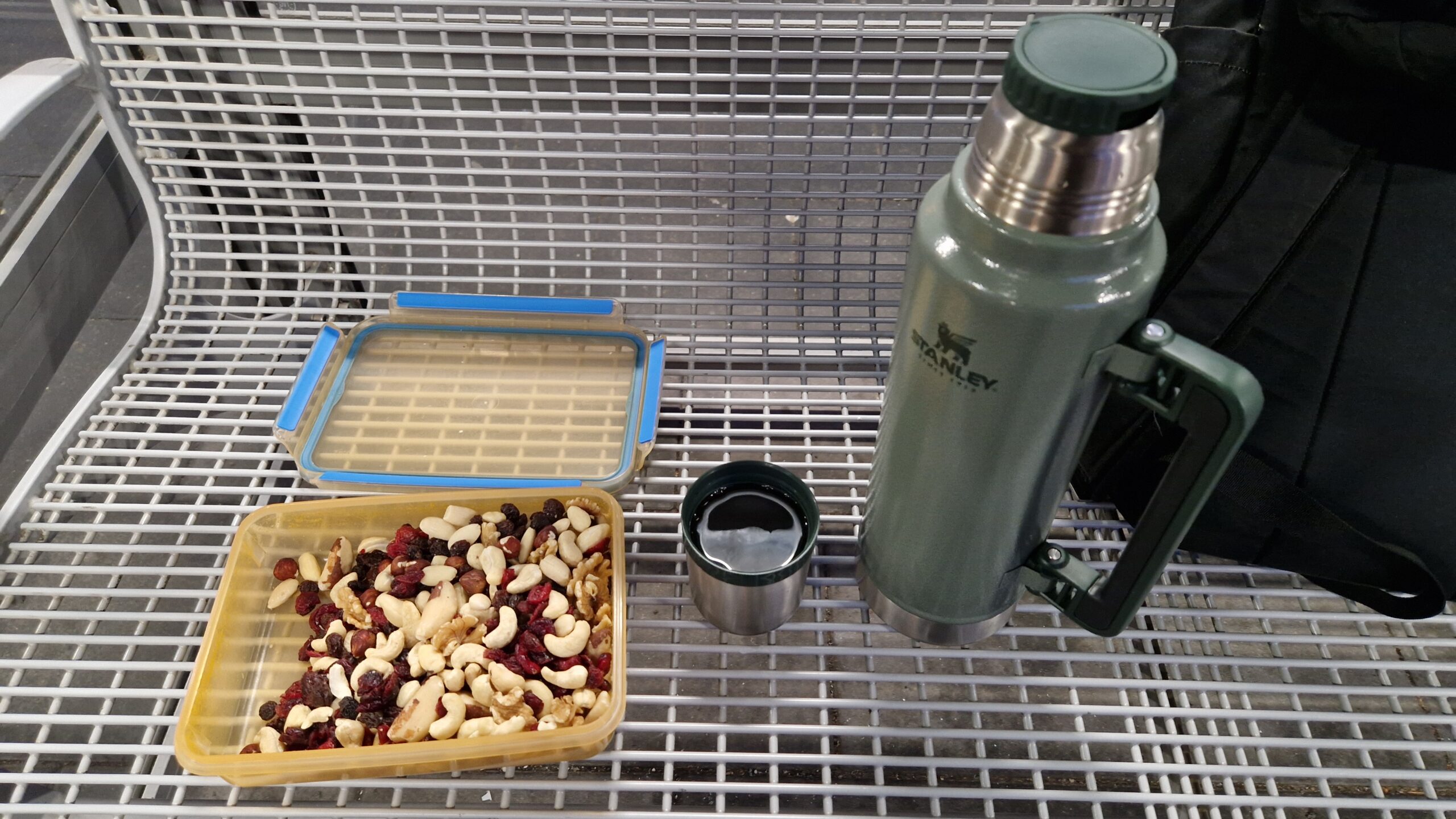
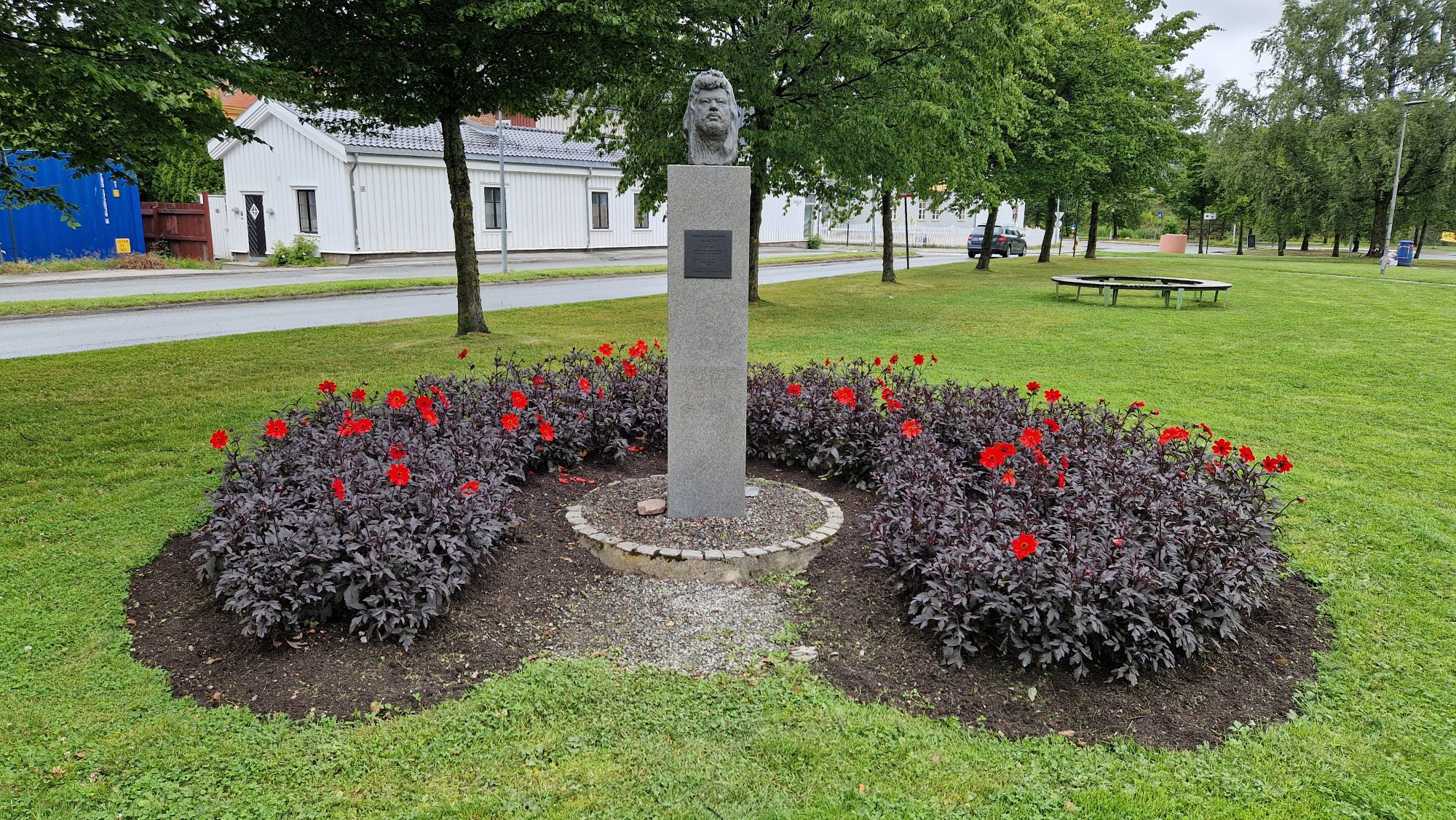
Coffee, nuts and berries! Everything a happy brain needs…
Happy New Year 2026 everyone! I hope you celebrated the new year’s holidays in peace with your families and friends. I’ve had some coffee and nuts, FeelsGoodMan!
As always, the year ahead looks ambitious. I plan to keep writing about my electronics projects, test equipment, precision measurements, and the tools that make all of this possible.
I’ve also noticed that I’m having troubles with writing blog articles for different reasons. One of my ongoing challenges is streamlining the writing process itself: keeping track of measurements, photos, schematics, revisions, and all the little iterative steps that never quite fit neatly into a finished article. Improving that workflow is a project of its own — but one that should make future posts clearer and more consistent. I also plan to use some “AI” or LLM-generated assistance text in order to overcome some “typically human” things like procrastination or writer’s blocks. This won’t compromise the integrity of my blog, because I don’t trust the current LLMs. There is currently no way around the scientific method or good scientific practices when it comes down to writing somewhat serious technical articles. Because this blog is mostly an “one-man-project”, I’m still dependent on your feedback as a reader. Please leave me an email if you find errors in my articles so I can correct them properly.
Unfortunately, I am always very busy and have little time for hobby projects. Time remains the most limited resource. Between work, projects, and everyday life, writing detailed technical articles is slow, but the intention for 2026 is very much to publish more than in 2025 — even if progress happens one careful step at a time. I’m aiming for 5…7 articles per year, depending on the topic and complexity of the article.
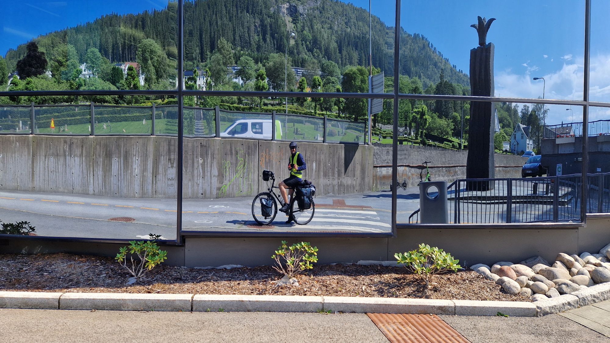
Outside of the lab, 2026 also comes with a bigger adventure: my second trip to Norway, continuing last year’s bike route from Bergen towards North. Long-distance bikepacking, combined with outdoor activities, camping, minimalism and self-sufficiency, fits perfectly with the spirit of this blog. I’m looking forward to sharing my travel impressions and lessons learned from the road.
Thank you for reading, experimenting, measuring, and building alongside me. May your probes be well compensated, your measurements stable, your antennas erected (in the best possible way) — and your projects successful in 2026.
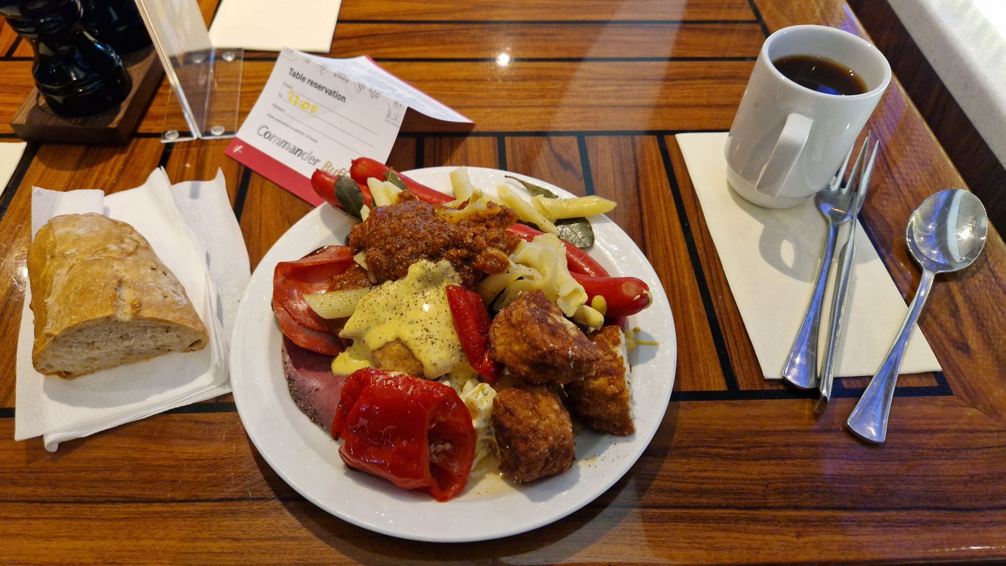
Merry day after Christmas everyone! I hope everyone is having a good time and doing fun projects during holidays and vacation. I’m trying to write a blog post again, so today’s blog entry will be about some of my efforts to recharge a battery! Can’t be that hard, can it?
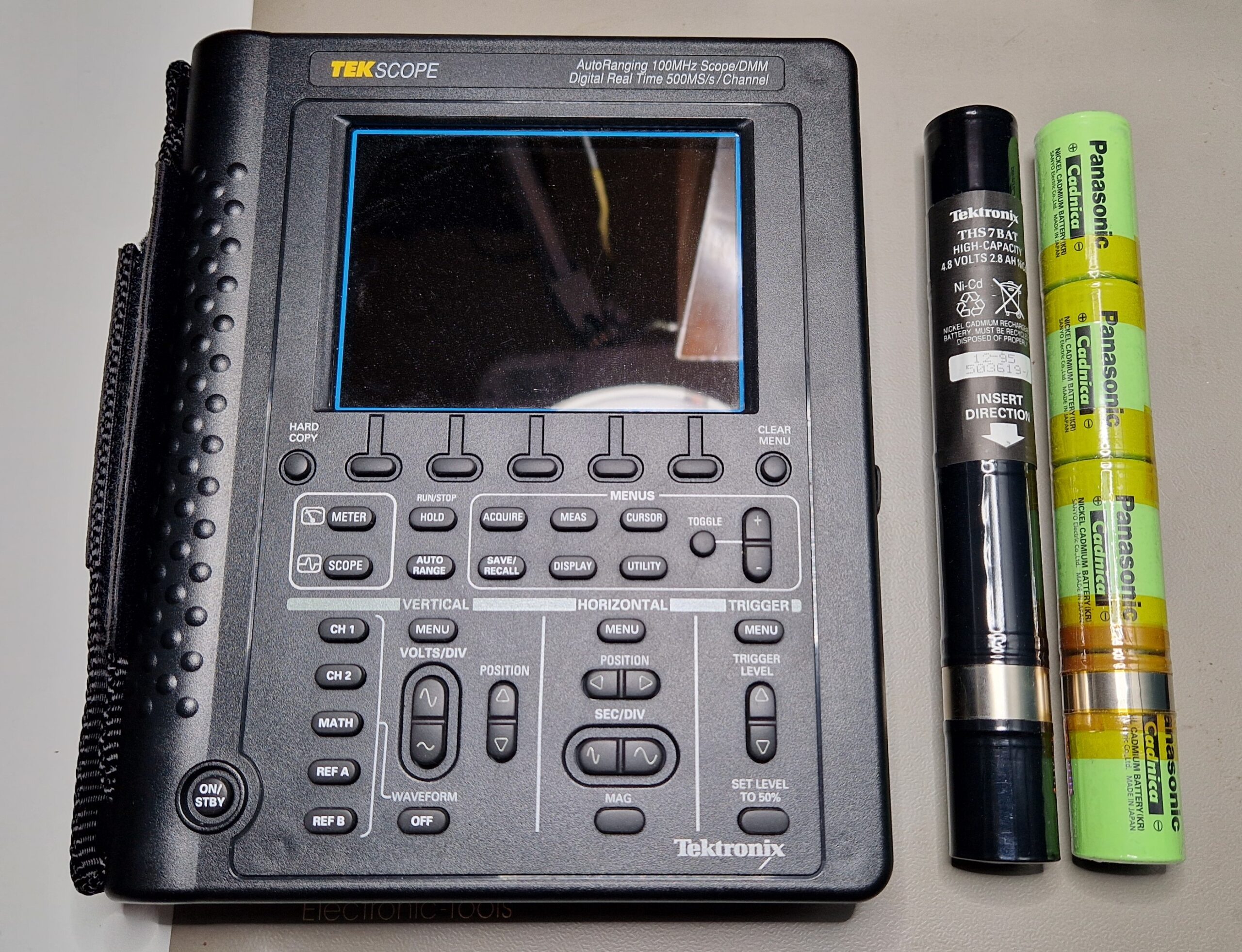
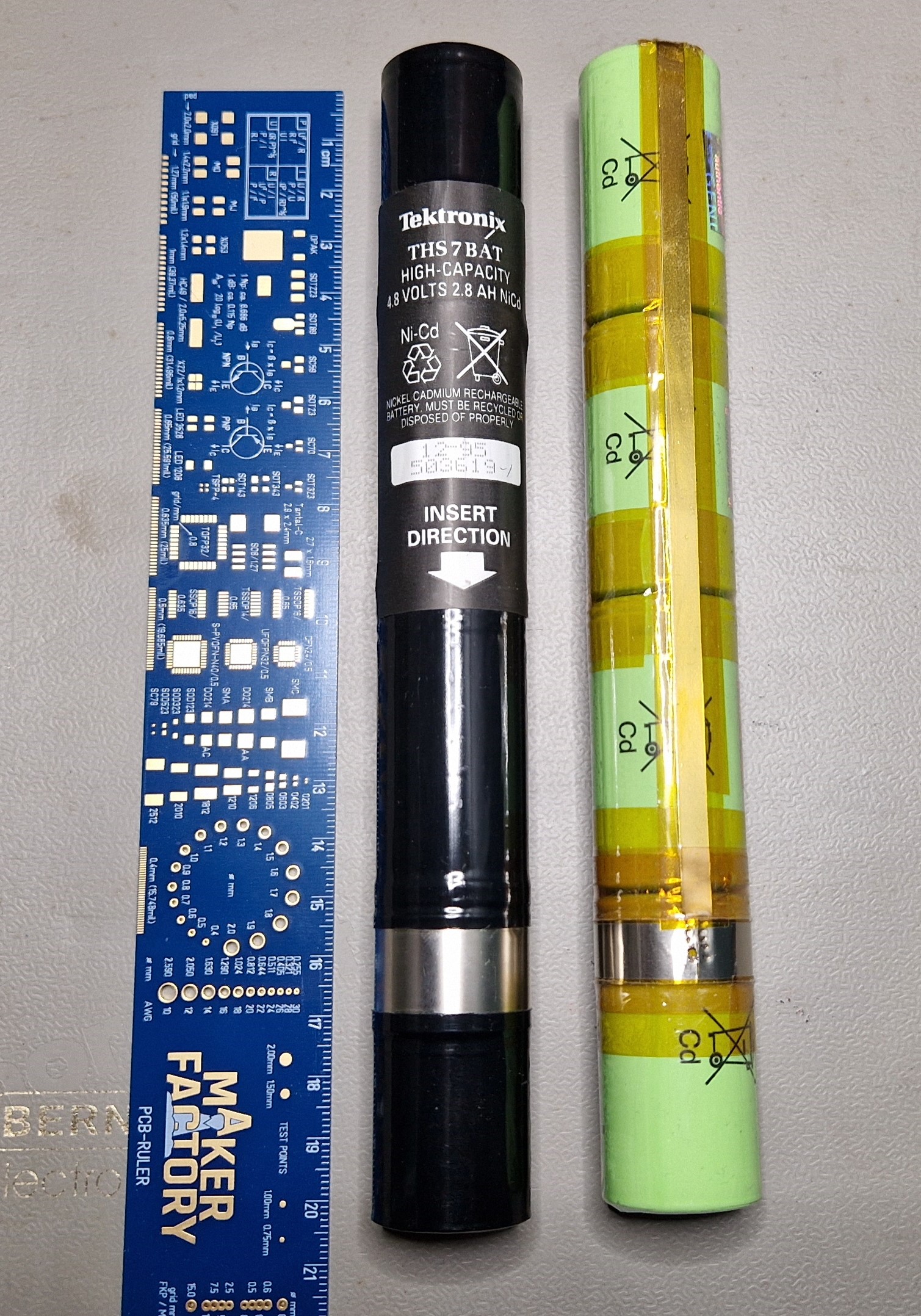
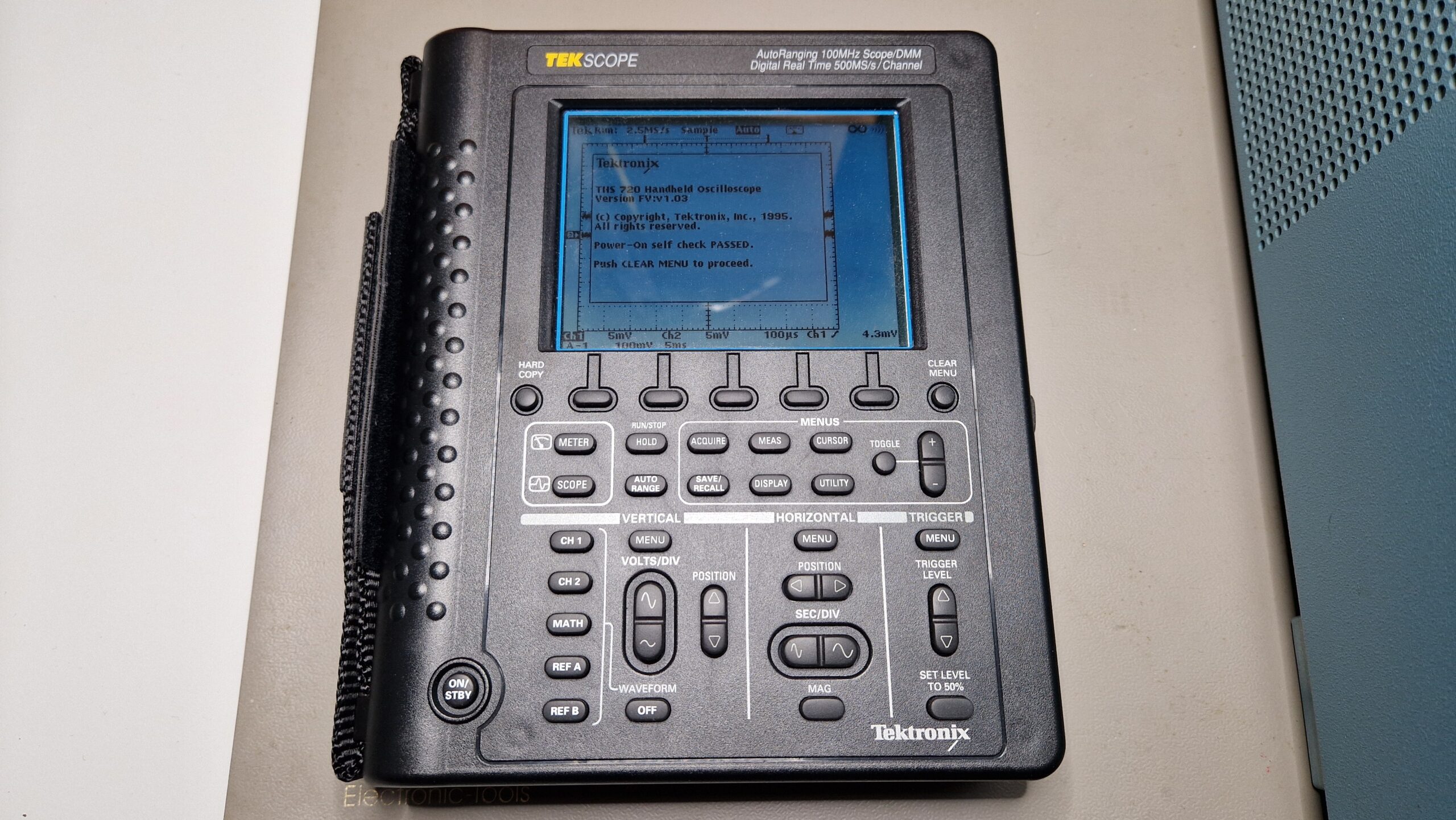
Tektronix THS 720 with rechargeable batteries. The original battery pack is labeled THS7BAT.
The Tektronix THS 720 is a portable and battery-operated 2 channel 100 MHz analog bandwidth, 500 MS/s oscilloscope with isolated BNC inputs and an integrated digital multimeter (DMM). It is a very useful tool for troubleshooting electronics or servicing (switch-mode) power supplies due to its isolated input channels. It can perform “floating” measurements and measure voltage differences safely on arbitrary potentials (similar to a handheld DMM). When testing switch-mode power supplies (SMPS, having a galvanic isolation and line voltages, e. g. 230 V) with an “ordinary” oscilloscope, keep in mind that the probe ground connector (GND) provides a direct and low impedance path to the oscilloscope chassis (mains earth referenced). This is potentially very dangerous, because if you connect your GND to a “floating” Device Under Test (DUT) at a higher voltage potential, the GND connector creates an electrical short between the DUT and the oscilloscope chassis. If the DUT and chassis are somehow connected through protective earth (PE), it can short out line voltages directly via your oscilloscope and perhaps ruin your day, too (danger of being electrocuted). In order to avoid these electrical safety dangers, the serviced DUT needs to be powered through an isolation transformer as a safety measure – or alternatively – it has to be probed by either using a high-voltage differential probe (for example Tektronix P5205A) or via a battery-powered, isolated (“floating”) oscilloscope (e. g. Tektronix THS 700 Series or Fluke ScopeMeter). There is an excellent explanation video on this matter from Dave Jones of EEVblog on YouTube.
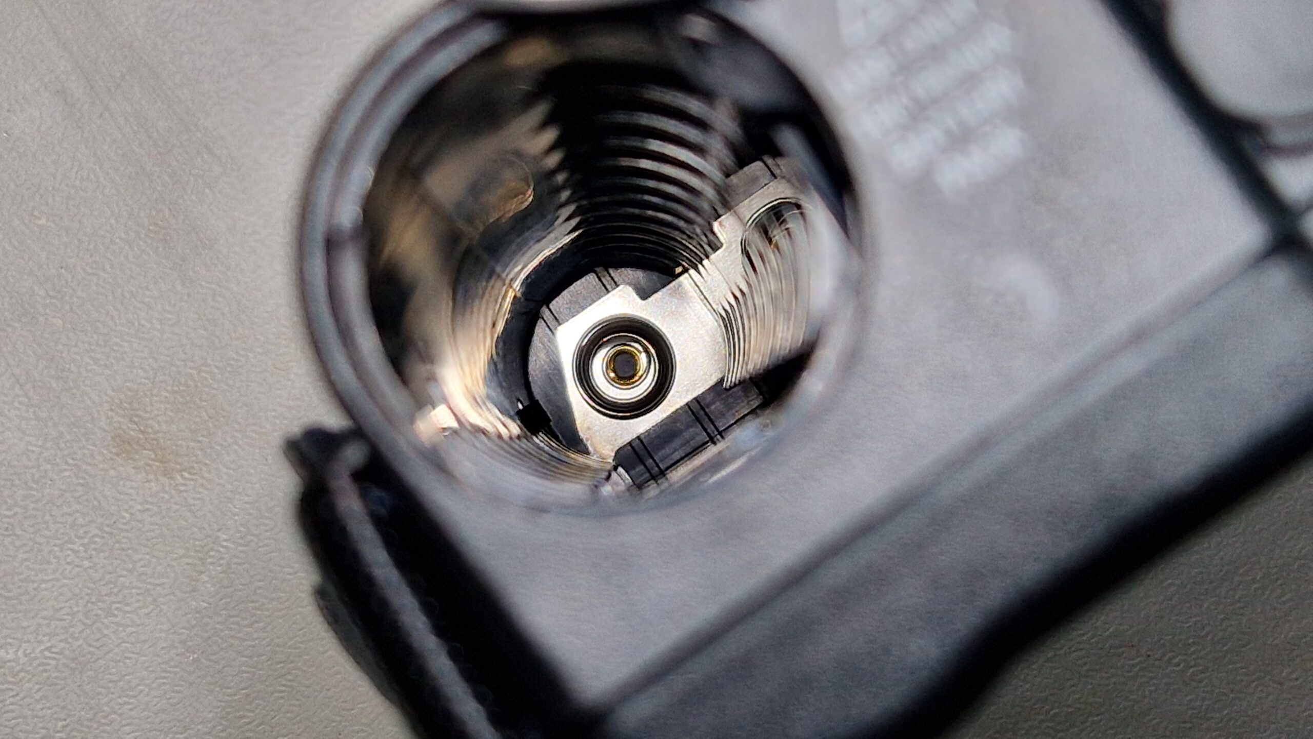
Isolated BNC inputs and DC supply input of the Tektronix THS 720Tektronix THS 720 battery compartment. The (+) electrode contact can be seen as a black square on the bottom left (around 7 o’clock)While powered on, the THS 700 Series oscilloscopes have quite a high current demand, which can be only supplied reliably by a Nickel-Cadmium (Ni-Cd) type of rechargeable batteries. Unfortunately, the Ni-Cd batteries have two disadvantages: they self-discharge over longer periods of time (at a rate of approx. 1% per day, it takes about 3 months for a complete discharge, inside of the scope they may discharge even faster within a couple of weeks) and they suffer to the memory effect (capacity deterioration due to charging/discharging cycles). I bought this oscilloscope for a very fair price (~200 EUR), however, with a dead Ni-Cd battery. The EEVblog users have investigated modern-era replacement possibilities such as NiMH batteries with special adapters which will fit inside of the oscilloscope battery compartment (length and diameter-wise). The alternative to this method is to buy certain Ni-Cd battery cells and combine them together into a battery pack.I was lucky to find an offer on Kleinanzeigen from a guy who already premade this kind of battery pack and I bought it from him for about ~50 EUR. This saved me a lot of time and tinkering because I didn’t have a spot welding machine in order to attach metal sheets to the electrode. So here is a comparison between the original THS 700 Series oscilloscope batteries and the DIY-type.
Comparison between THS7BAT and a DIY Ni-Cd battery packNi-Cd battery spot welding detail imageFour C-type cells (Panasonic Cadnica, model N-3000CR, Ni-Cd 1.2 V, 3000 mAh, Flat Top (non extending), diameter 26 mm, single cell length 50 mm, ~7 EUR/piece) were used and contacted in series and assembled with Kapton tape so they form a single battery unit. Unfortunately, the THS 720 oscilloscope demands the positive electrode (cathode) to be placed at a certain position along the battery axis – you can’t simply use the both ends of the batteries unless you want to modify your scope for this purpose. In order to meet the requirements, the positive battery electrode needs to be extended by spot-welding a thin metal sheet and connect it to a metal ring, located about 40 mm above the negative electrode (anode) of the bottom cell. The metal ring provides the positive battery supply connection to the oscilloscope. This is a very odd construction but that’s how the oscilloscope was made back in the mid 1990s. It’s important to notice that the metal sheets must be spot-welded to the battery electrodes in order to provide reliable electrical connections. Leads cannot be soldered to the battery electrodes directly for different reasons – if they come off, they can cause power loss or even shorts, the heat applied during soldering can also damage the battery cell. The metal sheet needs also to be sufficiently isolated with suitable non-conducting tape in order to prevent (potentially dangerous) battery shorts.
Ni-Cd battery cathode ring – detail image
Anyways, the Panasonic Cadnica replacement batteries turned out to work exceptionally well and provided enough power for a certain amount of time (depends on oscilloscope usage, perhaps 1 day with intermittent usage). I didn’t use the oscilloscope very much in the past and the battery was discharged as expected. In order to recharge the battery, I originally used the oscilloscope’s internal charging circuit, which “kinda” did the job. The charging at supplied voltage of 12 V and 1 A took around 24 hours. I noticed a significant heat-up of the battery packs up to ~45 °C, maybe 50 °C so I wasn’t quite sure about the unsupervised safety of this charging procedure. The max. charging temperature according to the datasheet is specified at +45 °C so I really hit the temperature limit. To avoid this in the future, I was looking for a fast Ni-Cd charger where I could quickly recharge the batteries without a significant heat build-up. There is a Tektronix THS7CHG Battery Charger on the 2nd hand market (e. g. eBay), however, it’s too rare and too expensive and not a viable option. An EEVblog user has constructed a similar charger with off-the-shelf components and 3D-printed housing. For a single Ni-Cd cell, the rapid charging time should be in the order of 1 … 2 hours at a nominal Voltage of 1.2 V and maximum currents of up to 4500 mA – compared to the 16-24 hours at standard charging currents (300 mA).
Robbe Power Peak Infinity 2 battery chargerRobbe charger, sitting on top of a switch-mode power supply during a charging operation
For this purpose, I bought a 2nd hand discontinued universal charger, which are very common in the fields of radio-controlled toys and RC models (drones, cars, boats etc.). It was manufactured by a German company called Robbe (type: Power Peak Infinity 2), which is capable of charging and discharging different types of batteries (NiMH, Lead Acid, Ni-Cd). In order to operate it, one needs a (switch-mode) power supply which provides the necessary voltages and currents for operation of the charger (e. g. 13.8 V and 0.1 … 5 A). The battery charger’s microcontroller monitors and regulates the output voltages and currents, which suits the charging profile of the batteries being recharged. In case of 4 Ni-Cd batteries, we need at least 4x 1.2 V = 4.8 V with a current limitation of 4.5 A (according to the Cadnica datasheet). The charging speed is limited by the battery temperature, the build-up of internal pressure and the so-called charge rate C. Typical charge rates are around 0.1 C while “fast” charge rates are around 0.5 C up to 1 C. Due to limitations of Ni-Cd batteries (memory effect, ~500 recharging cycles), they should be discharged first, then recharged at low rates (e. g. 0.1 C) to increase their longevity. For long-term storage of Ni-Cd batteries, Robbe user manual recommends to discharge them first and store them in a cold and dry place (e. g. in a fridge at 4 °C) in order to mitigate the performance deterioration due to the memory effect.
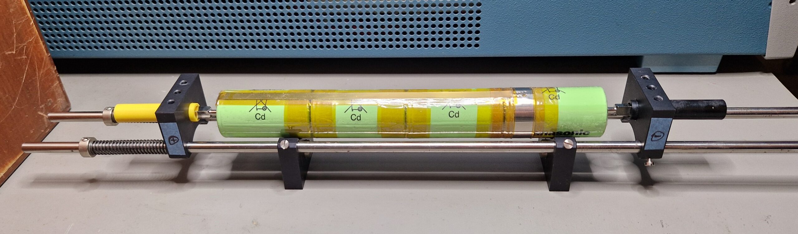
My experimental setup for battery charging and monitoring: Robbe charger, switch-mode power supply, Tektronix TDS 3034B oscilloscope with a P6139A probe and TCP202 current probe. In the center part of the image, the charging fixture for the Ni-Cd battery is shown. Not shown in picture: digital multimeter HP 34401A. Top left: Rubidium Precision Time Base (not used for this experiment, just casually laying around)Quick-and-dirty assembled Ni-Cd battery fixture from optics parts. The electrode contacts are just standard 4 mm banana plugs inserted into 4 mm banana couplings.
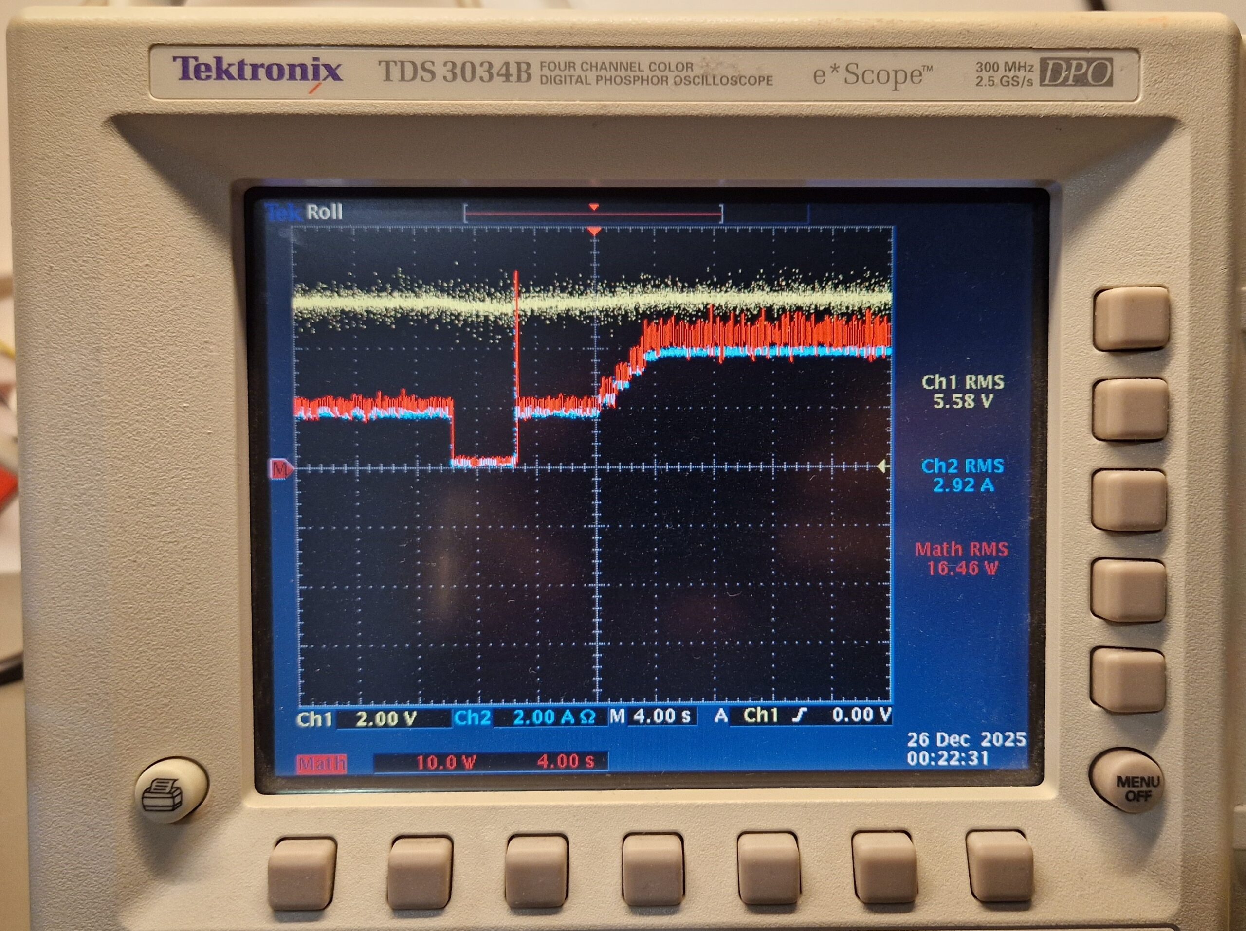
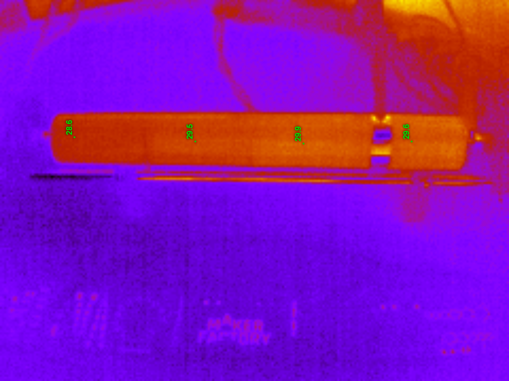
My charging/discharging setup looks as follows: the switch-mode power supply (JAMARA Germany DC Regulated Power Supply, Output: 13.8 V & 0-20 A) is connected to the charger. The charger output is then connected to the battery pack fixture. For my battery fixture, I used some spare optics parts I had at hand. The spring-loaded electrode helps to keep the battery in place and also helps to provide a reliable electrical contact. The recharger was powered on and set up to the “DISCHARGE -> CHARGE” mode, which is recommended by the Robbe manual. The battery under test had a remaining voltage of about 2.4 V and was discharged with a current of about 0.1 to 0.3 A. As soon as the battery was discharged to a certain threshold voltage (e. g. 1 V open circuit voltage), the charging cycle began by a slow ramp-up of the voltages and currents. After few minutes, the rapid charging is reached at approx. 6 V and 4.5 A (about 30 W), which corresponds to a charge rate of 1.5 C. I could observe some kind of a charge duty cycle, where the current flow stopped for a certain amount of time before continuing again – perhaps for thermal management purposes. The charging process took about 60 minutes, the estimated restored battery capacity (= transferred charge) was in the order of 3000 mAh. The temperature of the setup was monitored during the charging process with a thermal camera, however the battery pack didn’t heat up significantly in comparison to the mentioned THS 720 internal battery charger. The voltages were monitored by a digital multimeter HP 34401A and an oscilloscope Tektronix TDS 3064B, the current was monitored by a Tektronix TCP 202 current probe. This allowed me to estimate the power demand during the charging process.
Measured voltage of the empty Ni-Cd battery pack
Ongoing discharge, monitored via an oscilloscope
Charging ramp-up shortly after charging begins
Charging voltage, current and power at maximum output (6 V, 4.5 A)
Charging has finished
Thermal image (IR) of the experimental setup
Temperature measurement during Ni-Cd rapid charging
Thermal image of the battery setup, taken few minutes later
I was surprised how well and how fast this recharging process went. The DIY battery pack proved to be suitable alternative to the original battery pack Tektronix THS7BAT. Unfortunately, the Ni-Cd batteries age and need to be replaced over time. However, an inexpensive alternative with modern-day parts for a reasonable amount of money (~30 … 40 EUR) can be used to replace the original battery pack and extend the lifetime of the oscilloscope usage, at least until the internal electronic parts start to fail (e. g. the opto-couplers of this scope).
Tektronix THS 720, operational with a fresh recharged battery
My vacation has come to the end and I arrived safe and sound back home in Braunschweig, Germany. Everything went well and it’s time to reflect the past four weeks and draw an outline for the bike tour in summer 2026.
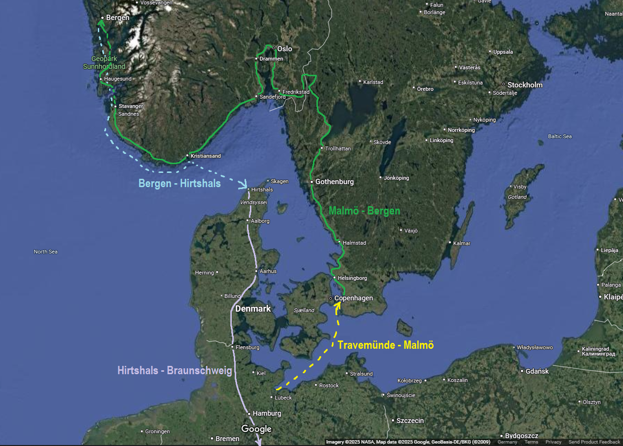
My Bike Tour 2025 from Malmö (Sweden) to Bergen (Norway) – a total distance of 2120 km in 22 days! Source: Google Maps
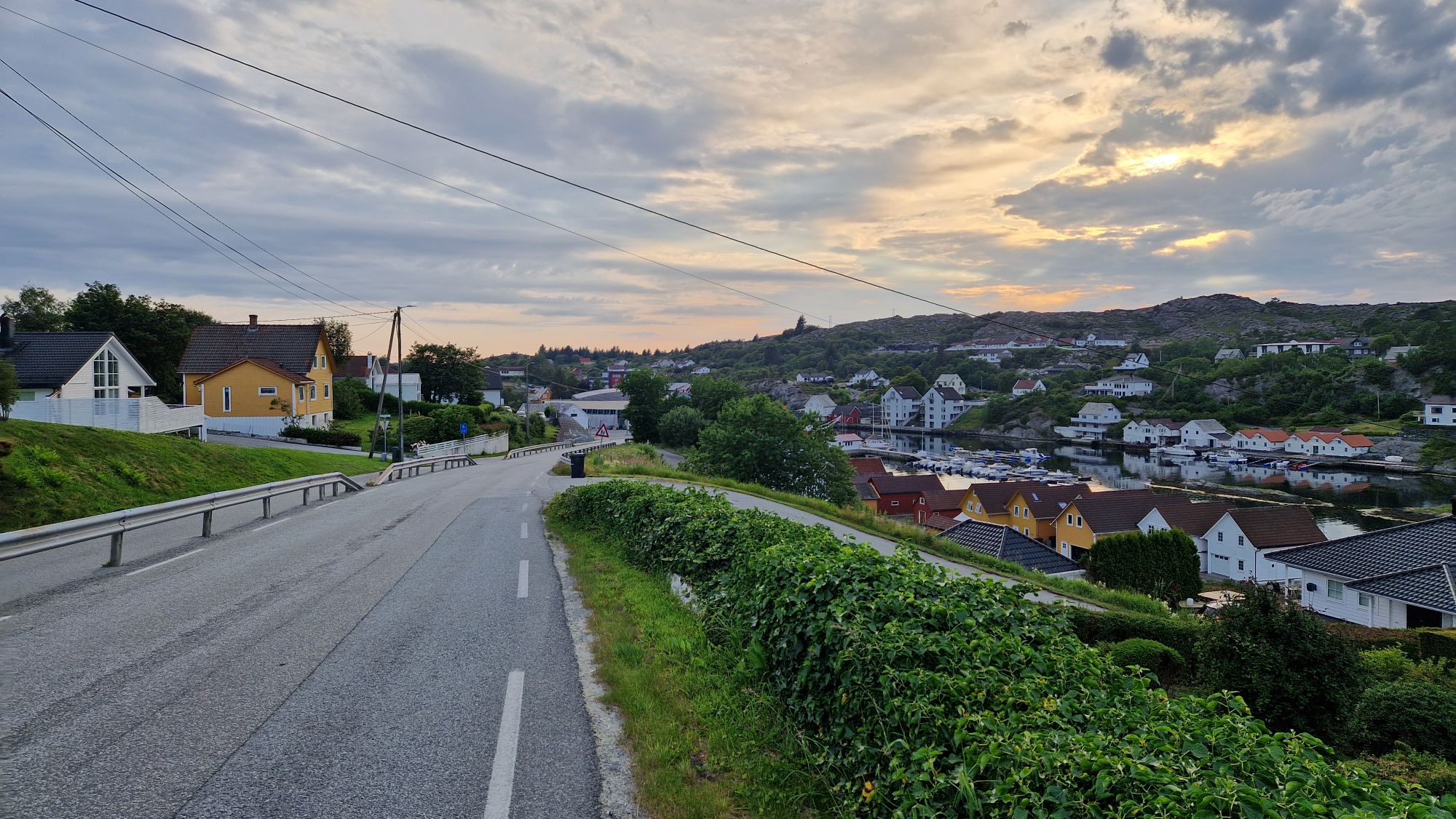
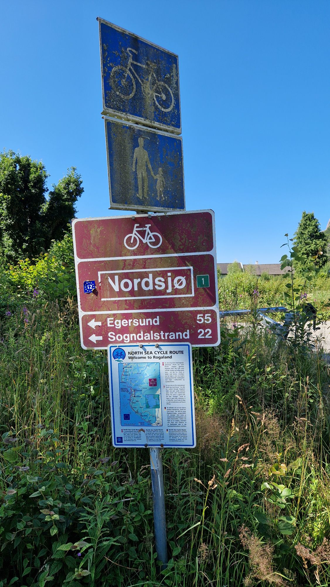
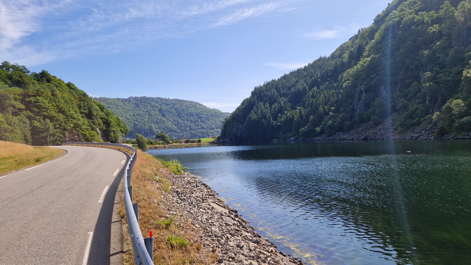
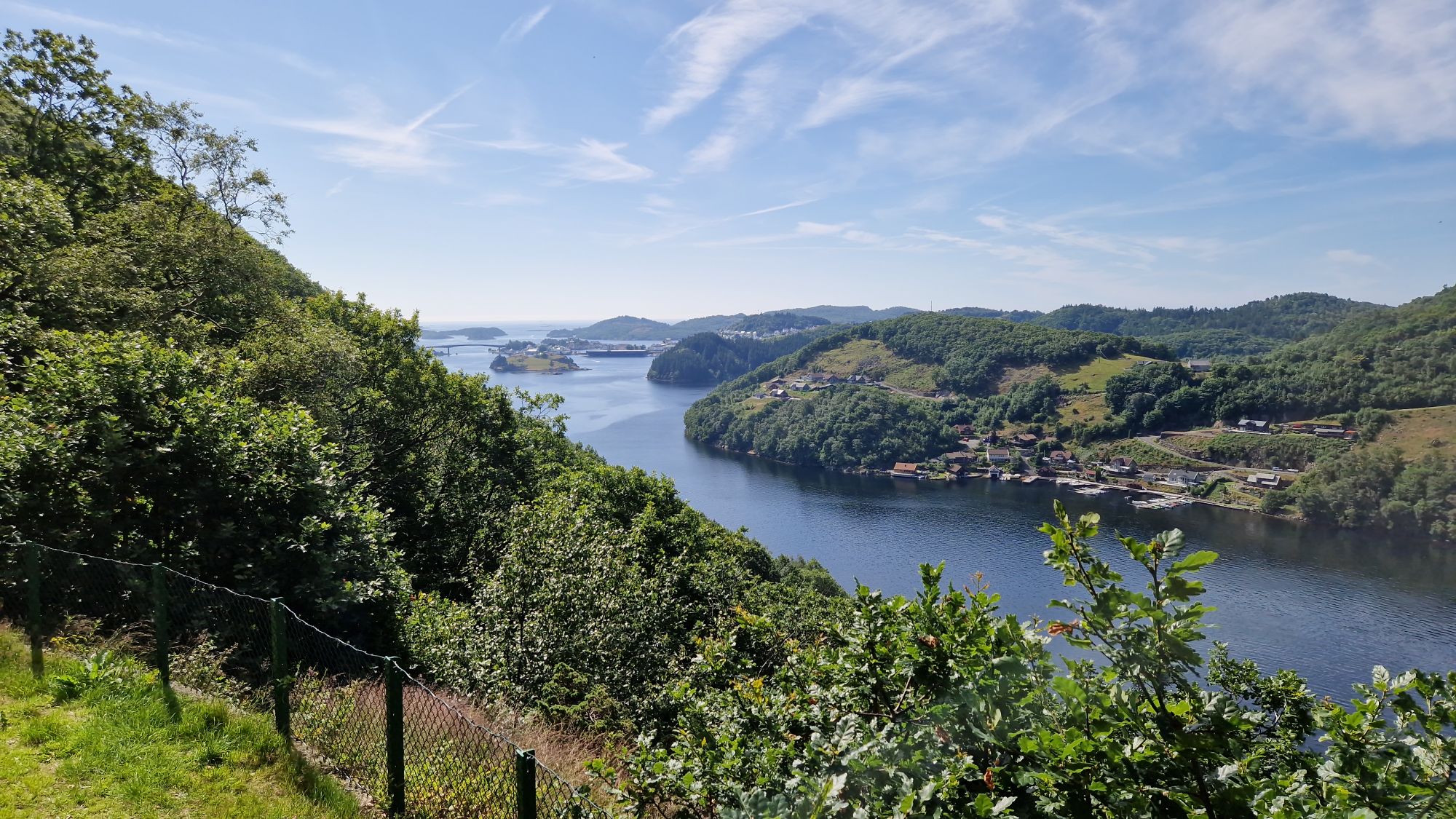
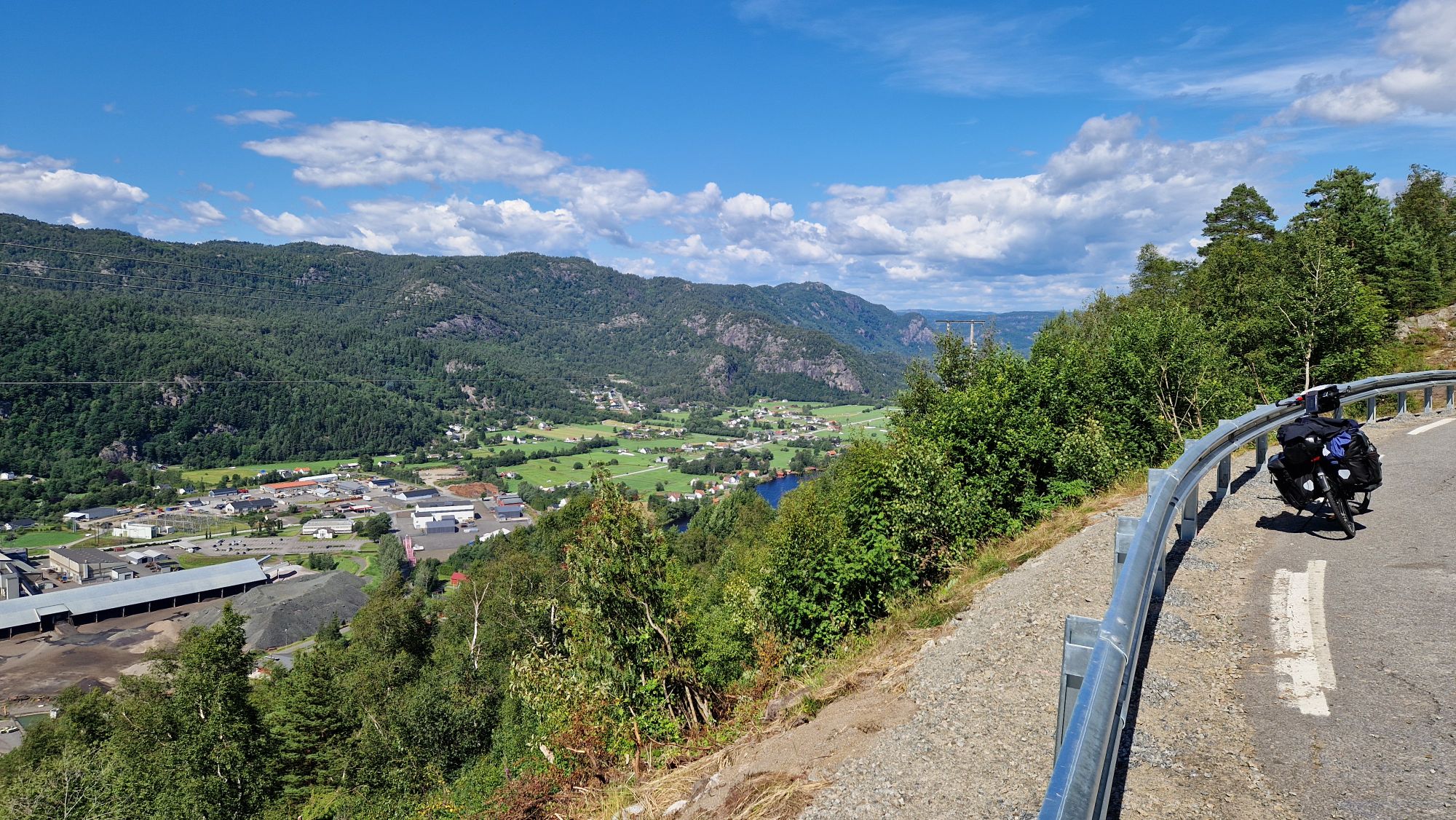
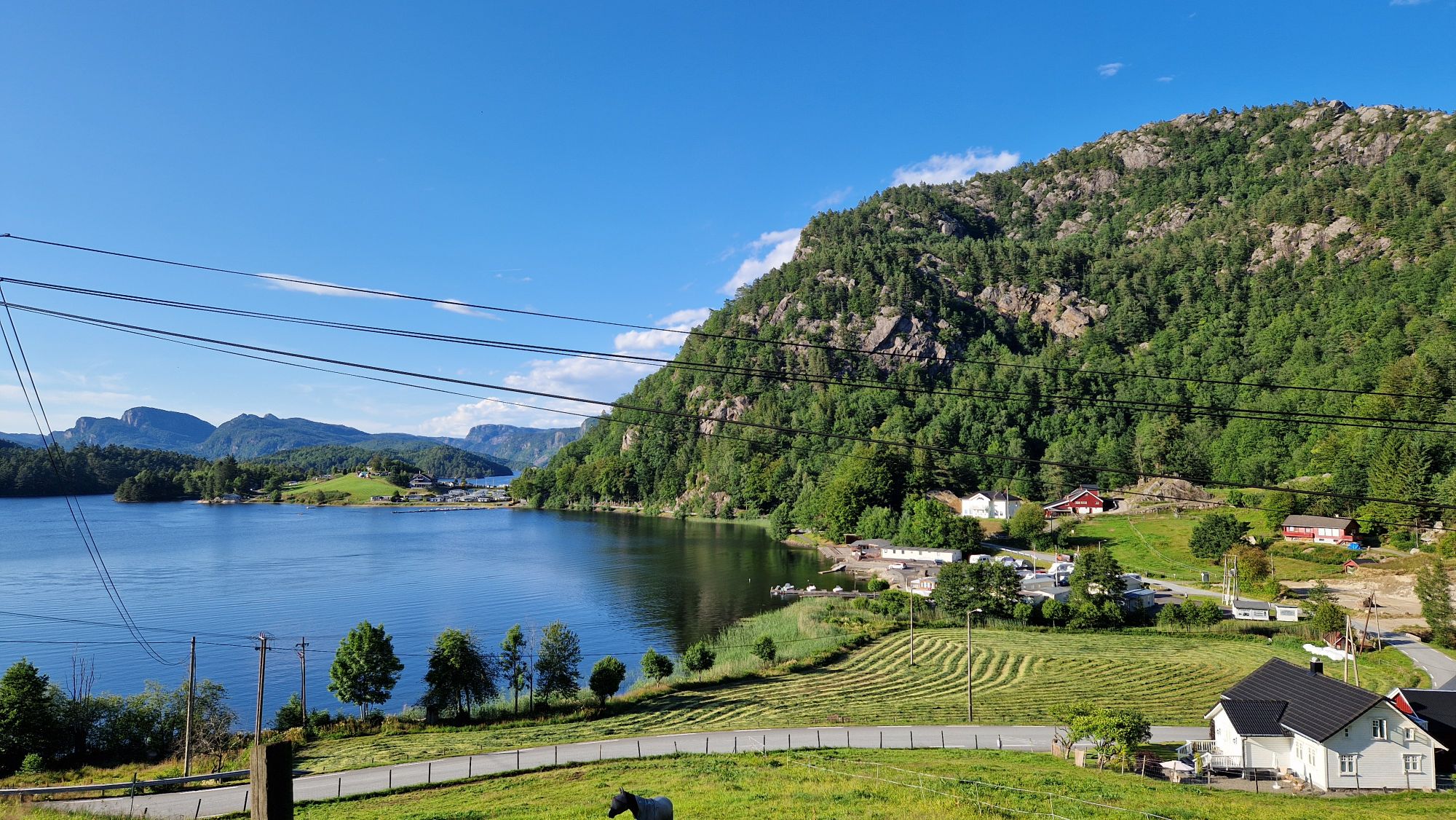
This was one of the best tours and vacations I ever had. I’ve cycled the Scandinavian leg of the North Sea Cycle Route No. 1 – around 2120 km (= 1317 miles) in 22 days from Malmö (Sweden) via Helsingborg, Halmstad, Göteborg, Vänersborg, Mellerud, Bengtsfors, Töcksfors, Ørje (Norway), Halden, Fredrikstad, Oslo, Drammen, Tønsberg, Langesund, Kragerø, Arendal, Grimstad, Lillesand, Kristiansand, Mandal (at midnight), Lyngdal, Farsund, Liknes, Flekkefjord, Egersund, Ogna, Stavanger, Haugesund, Leirvik, Bergen and many more in-between cities. The weather was perfect for cycling – mostly sunshine or friendly with occasional rain, I liked and enjoyed the lakes, the sea and the landscapes. I’ve met wonderful, kind and like-minded people along my route.
I’ve tried to document my voyage in daily blog posts. There was an overload of so many impressions almost every day! So I tried to keep up with the happenings on road. Thanks to the very good cell phone connections along the route, I was able to do it in a minimalistic fashion on my smartphone. I’ve made over 3000 pictures and it was difficult to make a good selection, because almost every picture has its own story… I hope that some future-travellers will find those information useful to plan their own route. If you have some specific questions about this bike tour, please write me an email at DH 7 DN [at] darc [dot] de. I’m checking it on a weekly basis due to low traffic – but I’ll answer asap!
Training my legs
The preparations for this particular tour started in winter 2024/2025. I’ve been doing cardiovascular training during the winter/spring months and basically cycling on average 5-6 days per week. I was able to reduce my weight from approx. 100 kg to about 92…94 kg in order to get in shape. The training was nothing special, just the “usual” 60 minutes or 25 km of fast cycling per day. I’ve tried to keep it up with the training plans just two days before the journey started.
Planning the tour
I started planning this bike tour on paper in February/March 2025. The main inspiration came from the German website Radreise-Wiki / Nordseeküstenradweg Norwegen and the OpenCycleMap.org website. It was a very good guide what to expect, huge thanks to the creators and writers of the wiki and the map. However, there is no “recipe” for such a week-long journey – one has to pick out suitable tracks. It’s impossible to see everything in a limited amount of time. So I’ve done some research on the internet (Google for bike tours to Norway), watched some YouTube videos (can highly recommend Bicycle Touring Pro YouTube Channel), checked the Wikivoyage for possible tourist spots and few others. A fellow cyclist showed me a nice travel guide booklet for this route, which I didn’t have on my mind. Anyways – much time went into preparation and creation of a plan or “time schedule” in order have a “tailored” bike tour. You can try to do it “by the numbers” but be aware of some possible real-life obstacles.
However, the route planning on a computer looked very easy but was hard to execute on-site. I’ve miscalculated the distances with errors of as high as +30%. For example: a 100 km daily cycling distance estimated by the map tool proved to be 120-130 km at the end of the day. I didn’t have experience with hills and what average speeds to expect. Now I’ve got some data for future tours… terrain with hills: 10-11 km/h on average, flat terrain: 14-16 km/h on average. It is easy to be wise after the event!
The previous bike tours to Denmark helped me a lot to estimate the travel effort. Having some knowledge Denmark’s roads, terrain, people, accommodation and railways made it much easier for me to travel. The first two days at Malmö/Copenhagen proved to be necessary, because starting such a tour on arrival would have been rather difficult: preparations and packing all the stuff took me about three full days and the immediate journey from Braunschweig to Travemünde via regional trains was very stressful. One has to calm down a bit in order to get in the mood and start a bit relaxed.
Starting the tour
The first three to four days on route are usually used for adaption to the new country and terrain. Trying not to overstretch, getting a healthy routine and finding out the right speed are the primary goals. If anything hurts – no problem, as long as you don’t ignore it and try to overcome it with painkillers. I had some problems with my toes on the feet during the first couple of days. I took care of it and it was gone. Getting a healthy amount of sleep (6-7 hours) every night was very important for the cycling performance. I was able to cycle 100 km per day on a constant basis, sometimes 120-130 km per day were possible without having pain in my legs. That kind of performance was necessary, otherwise the planned schedule would have been in vain.
Riding a bike with too much weight
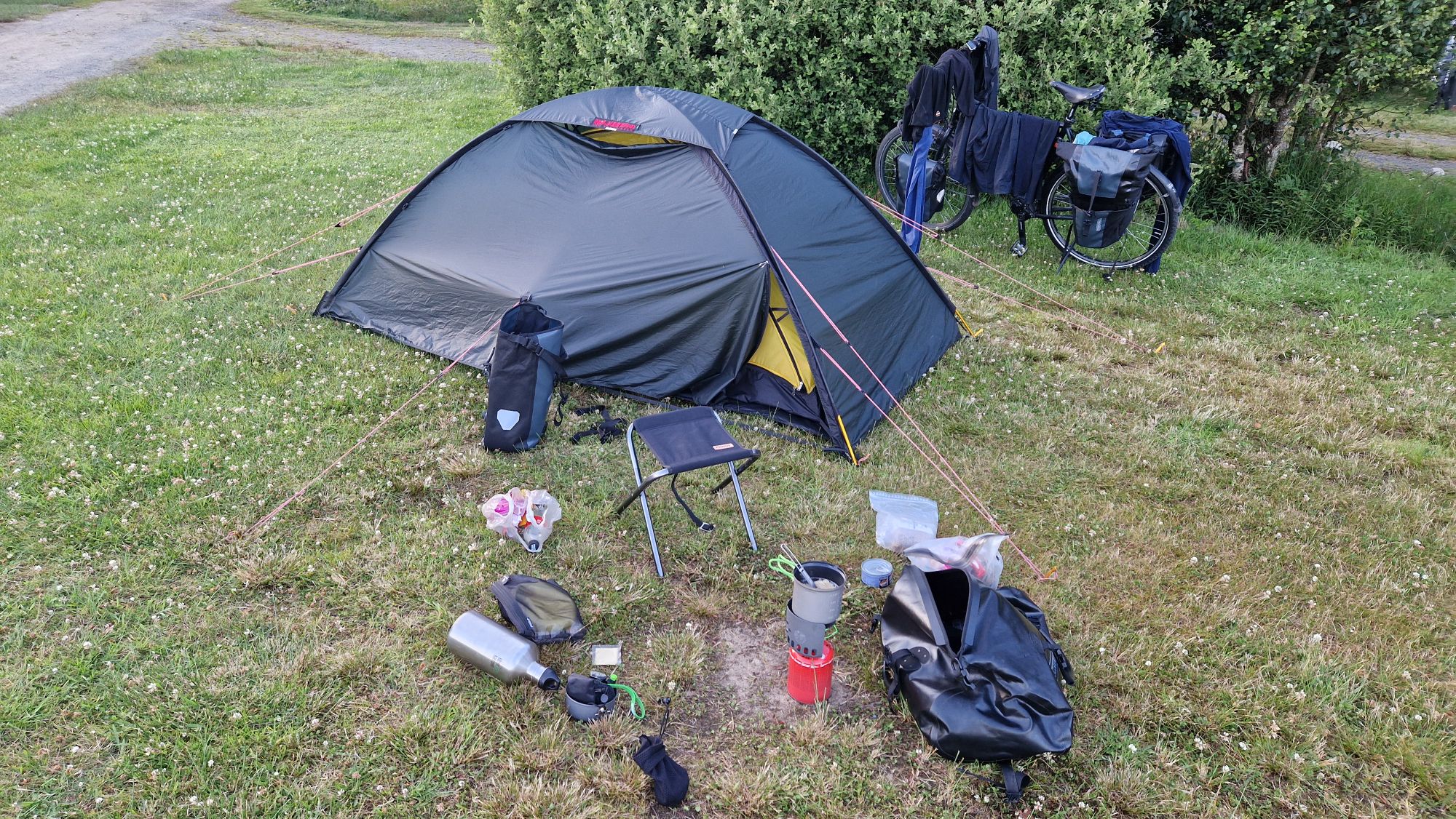
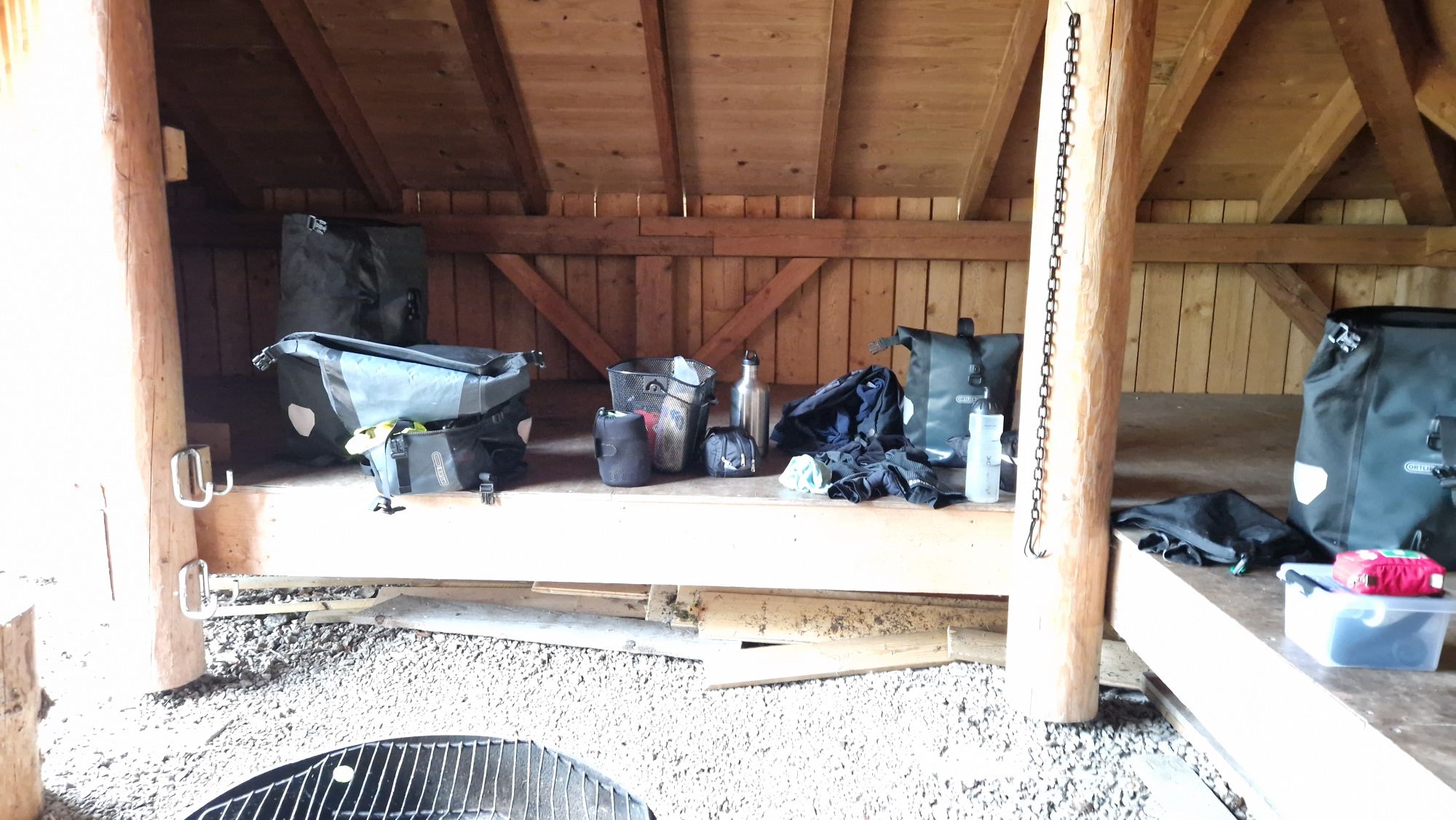
One major problem I had on route was a too heavy bike. The bike itself has some 18 kg. The fully packed pannier bags add some 25 kg, water and food may add another 10 kg of additional weight. So the total weight of me including the fully packed bike was up to approx. 140 to 150 kg! I always travel too heavy but this proved to be extremely difficult in the hills of Norway. I had to push my bike uphill a lot and tried to shed some weight by carrying a bit less food and water. I was considering of sending stuff back to Germany by mail but luckily it wasn’t necessary. I’ve carried a lot of unnecessary or unused stuff, such as backup clothing (“just in case” but the “case” came maybe with 5% chance), portable fan (for hot nights inside of the tent), a camping chair (used it only 3 times, great for full trains with no free seats), a basket (to keep the pannier bag in shape, worst decision ever), two steel bottles (for extra water, were sometimes useful but took too much space in the bags) and some other gadgets/tools (bags, tent pegs, USB cables, rags, …). The weather proved to be very favorable at 15 °C during nights and 20…25 °C during days. I’ve used my sleeping bag on three occasions in some shelters but most of the time I have used the Merino Wool Sleeping Bag Inliner as a “sleeping bag” inside of my tent. If it gets a bit colder at night, one can put on some additional clothes to stay warm, otherwise no “classic” sleeping bag is necessary. This can save up a lot of precious weight and volume and make life a bit easier.
For the future travels to Norway, I would have to lose some weight (down to 80…85 kg) and shed some equipment to get down to ~130 kg of total weight. This would improve my cycling experience a lot.
Bike performance, maintenance and technical difficulties
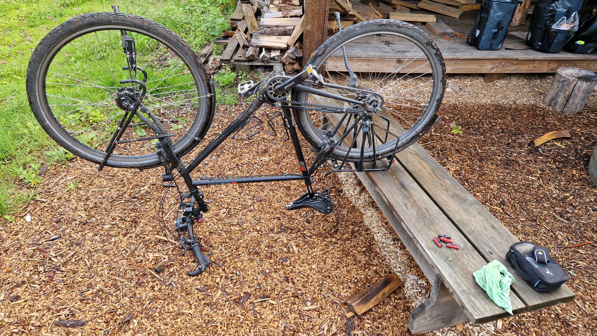
About 6 weeks prior to the tour, I’ve let my bike workshop inspect my tour bike, the vsf Fahrradmanufaktur TX-1200. They have replaced the front wheel, the pedals (both had worn-out bearings) and brake pads. Besides that, everything else looked fine. On route, I’ve had two flat tires on the back wheel due to riding a very heavy-loaded bike on coarse gravel roads. The little tiny and sharp stones sliced the tire over time and pointy shards were able to puncture the hose. I’ve replaced the tire and hose and had no more problems for the final ~300 km of the route. Another difficulty arised with the Pinion P.18 gear under heavy loads in combination with steep roads. Pinion is just great – I like it very much. It has some awesome properties I don’t want to miss anymore. However, when riding a 140 kg bike uphill in 10-15% slope in the 1st or 2nd gear, I’ve noticed some randomly occurring slippage, which is generally a bad sign. In order not to damage the Pinion gears, I’ve been cautious and pushed the bike uphill instead, some 20-50 meters before resuming the pedaling. There were no issues on flat terrain or hills up to 7% slope – lucky me. I’ll ask my workshop to look into this during the next inspection. Just be aware of the huge torques on steep roads – such conditions can easily damage any type of gear system (e. g. Roloff or Derailleur).
I’ve performed some minor maintenance on my bike during the tour. My Brooks saddle was greased every week due to heavy moisture (sweat, salt, rain). It’s necessary to keep the saddle dry and clean, otherwise it will start losing its shape or build up some cracks in the leather. The Brooks saddle was very comfortable and I could sit on it 8 hours per day without having soreness (however, try to change the sitting position every 20-30 minutes to relieve the buttocks, otherwise you will get a sore ass). It was necessary to replace brake pads once due to excessive breakings in the hills. The salty sea water spray caused some visible corrosion which needs to be taken care of. Besides that, I’ve greased the Gates belt every 200-300 km with the recommended spray. Some screws got a bit loose so I tightened them occasionally. Other than that, no further bike service or maintenance was necessary.
Camping, daily expenses and Allemannsrett
As I traveled with bike and tent, I spent most nights on camping sites or another places such as benches, shelters, forest and a parking lot. I took a two day stay in a hostel in Copenhagen but besides that, it was mostly camping. The camping prices in Sweden were moderate (20-30 EUR per person and night) and got really expensive in Norway (30 EUR per night, Oslo: 50 EUR per night). In Germany, a camping overnight usually costs between 15-25 EUR per person and night. So avoiding camping sites in Norway was necessary to stay in budget. Why? Because everything else is expensive, too! The food prices are also roughly 30% higher than here in Germany so it’s virtually impossible to keep the budget low if you plan to eat at restaurants. I’d estimate 30-40 EUR per person per day as realistic, however, the costs can double easily with “luxury food” and “premium services”. Other expenses such as transportation costs (by bus, ferries, trains, …), luxury money (eating at restaurant, having an ice cream) or emergency (repairs, replacement of equipment) should be considered in the price range of 300-500 EUR. I’ve spent around 400 EUR per week (= 60 EUR per day) on average and had around 600 EUR of travel expenses (trains, ships) in total. I could have saved some 20% by not buying stuff at gas stations or buying luxury food such as expensive chocolate bars… anyways, I think it’s fine.
The Allemannsrett I’ve expected was a bit different from what I’ve found on route. I’ve found many privately owned properties or signs with “Camping forbidden” where you aren’t allowed to camp over night. Those were exceptionally present along the touristic spots and along the Route 1. About 10 km outside of a town, and perhaps some few kilometers off-route, one could find very nice and appealing camping spot – perhaps at a lake. However, this heavily depended on the region and terrain. I couldn’t take my bike on steep hills or find a camping spot in a bush. The mosquito plague wasn’t as bad as expected. I was visited by them but sleeping in a tent helped a lot. I had some luck with pecks (killed them before they could bite me) and inspected my body two times per day for any intruders or parasites. The insects aren’t our enemies (except mosquitoes), they are just looking for a food source and being lured by our presence (e. g. breath, scent, noises). The bushcrafters on YouTube can give you some tips how to behave correctly in the forests and how to deal with the insects. Just be aware of this – better be safe than sorry.
Roads and traffic
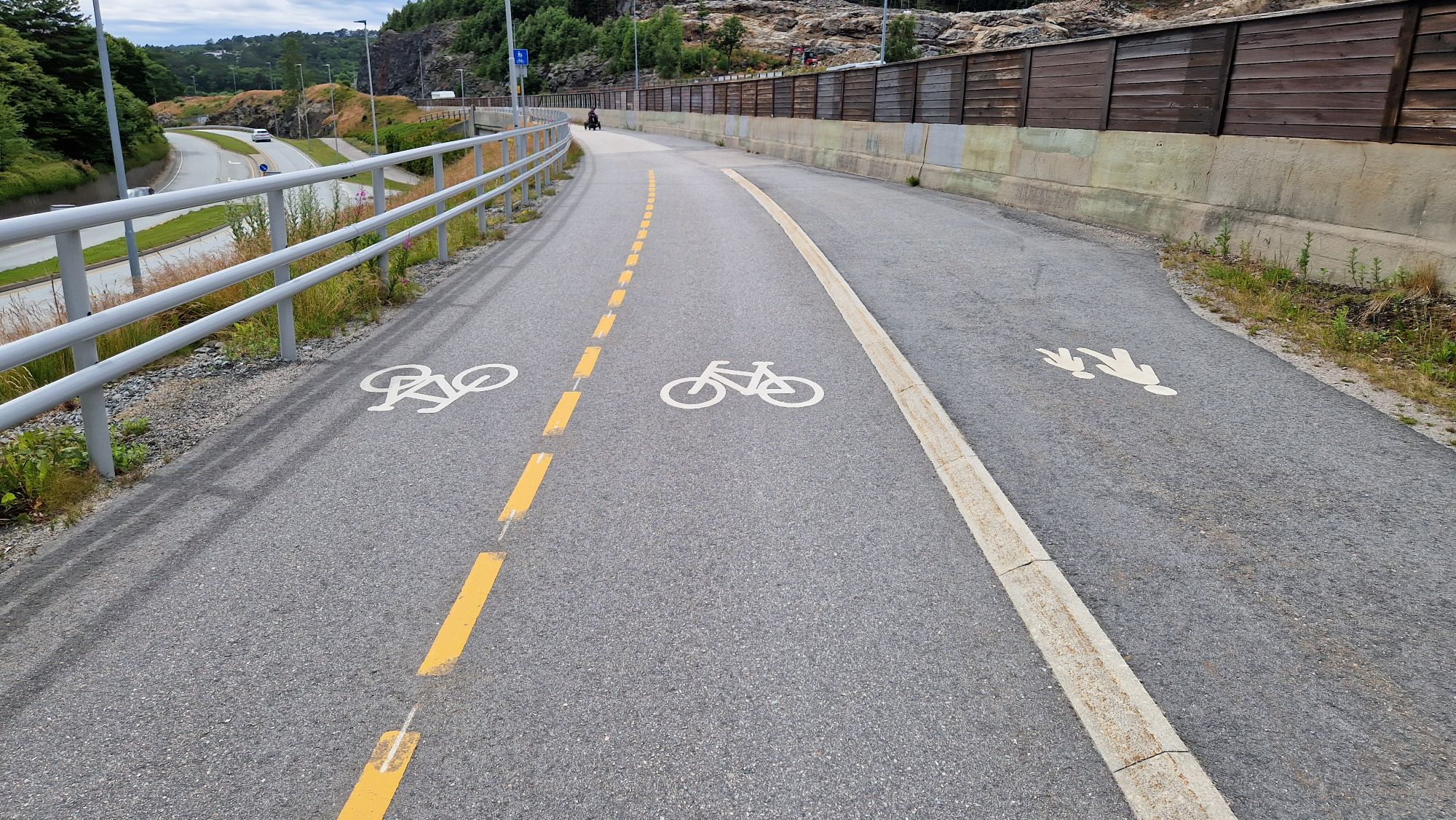
95% of the cycling roads in Denmark, Sweden and Norway were in an exceptionally good condition. I’ve never had such a good riding experience. The car drivers were very kind and cautious. They were overtaking cautious with about 1.5 meters of distance to me. I was warned by horn on three occasions: once by an Italian camping van driver, once by some crazy/drunk gang having a good time and once when I entered a tunnel where cyclists and pedestrians were not allowed. I felt safely on the roads and was very confident that I would finish the tour alive
On the other hand, there were some minor issues on route: missing signs put me on wrong route multiple times per day. Some construction sites (e. g. near Oslo) made a detour necessary. The ferries were great except that one in Øysang. I’ve noticed that many Swedish and Norwegian pedestrians walk on the “wrong side” of the road. This confused me a bit because I wasn’t used to drive on a collision course with a pedestrian. One just needs to signalize an overtake with the left arm and everything will be fine. Absolutely no need to bell and yell at them!
What’s next?
My wallet needs to heal. Usually I spend 600-800 EUR for such a three-week bike tour but this tour was expensive for sure. I’ll try to find a good compromise between travel expenses, accommodation and “premium stuff” next year. My next year’s journey would continue from Bergen to the north towards Lofoten. Lofoten aren’t a “cycling paradise” due to its mountain-like terrain and harsh weather conditions, however, I’d like to travel to the northern parts of Norway and perhaps reach Nordkapp by 2027. That would be awesome! The return route would be either by ship (Hurtigruten) or by train/by bus. I’d use more ferries to deal with crossing the fjords and try not to cycle on roads or through tunnels “by any means necessary”. Unfortunately, my vacation time is limited every year to 4 weeks during the summer time so I’d expect some 1500 km in 3 weeks at best with one additional week for arrival and departure. Right now, I’m just enjoying the good time I had in Denmark, Sweden and Norway and looking forward to return next year…
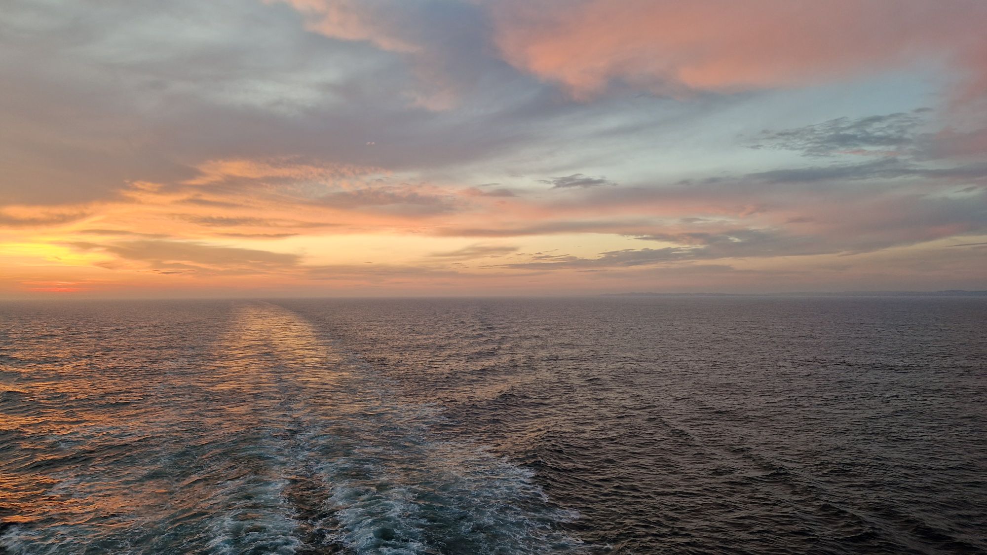
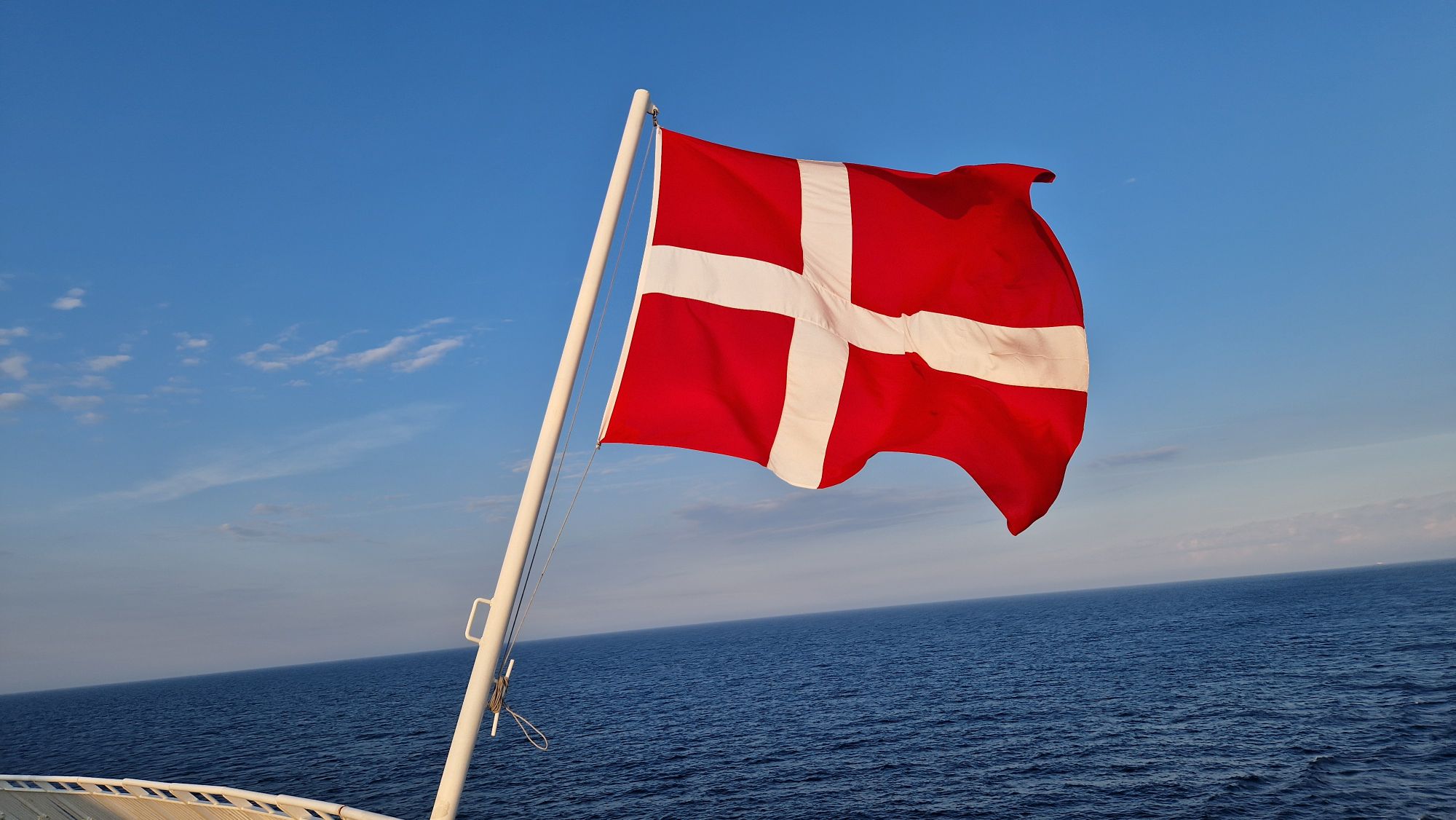
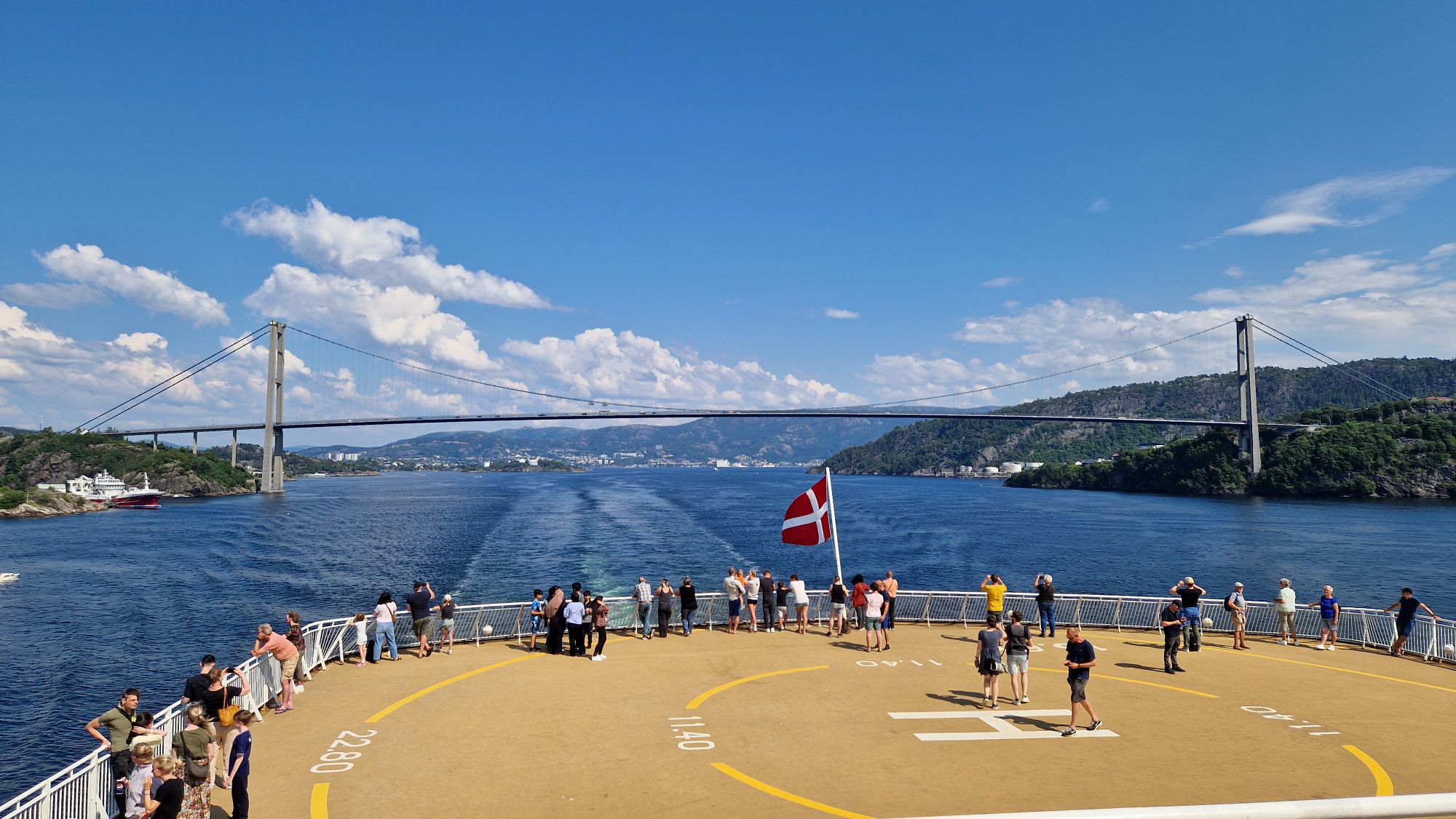
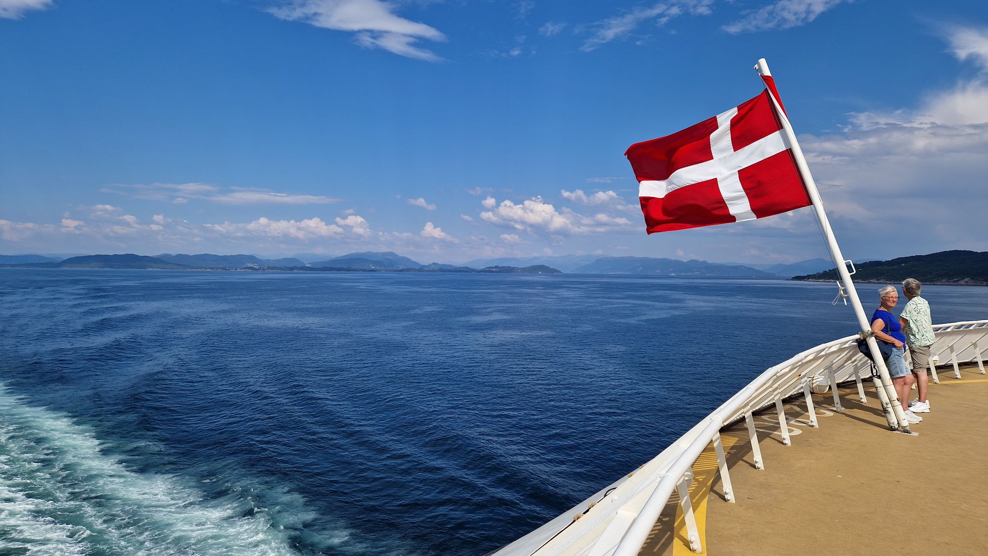
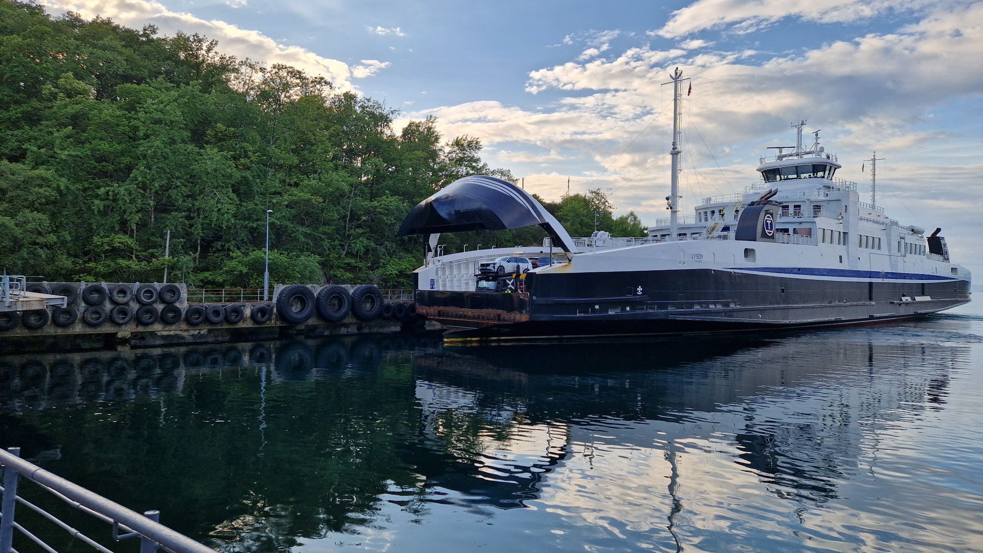
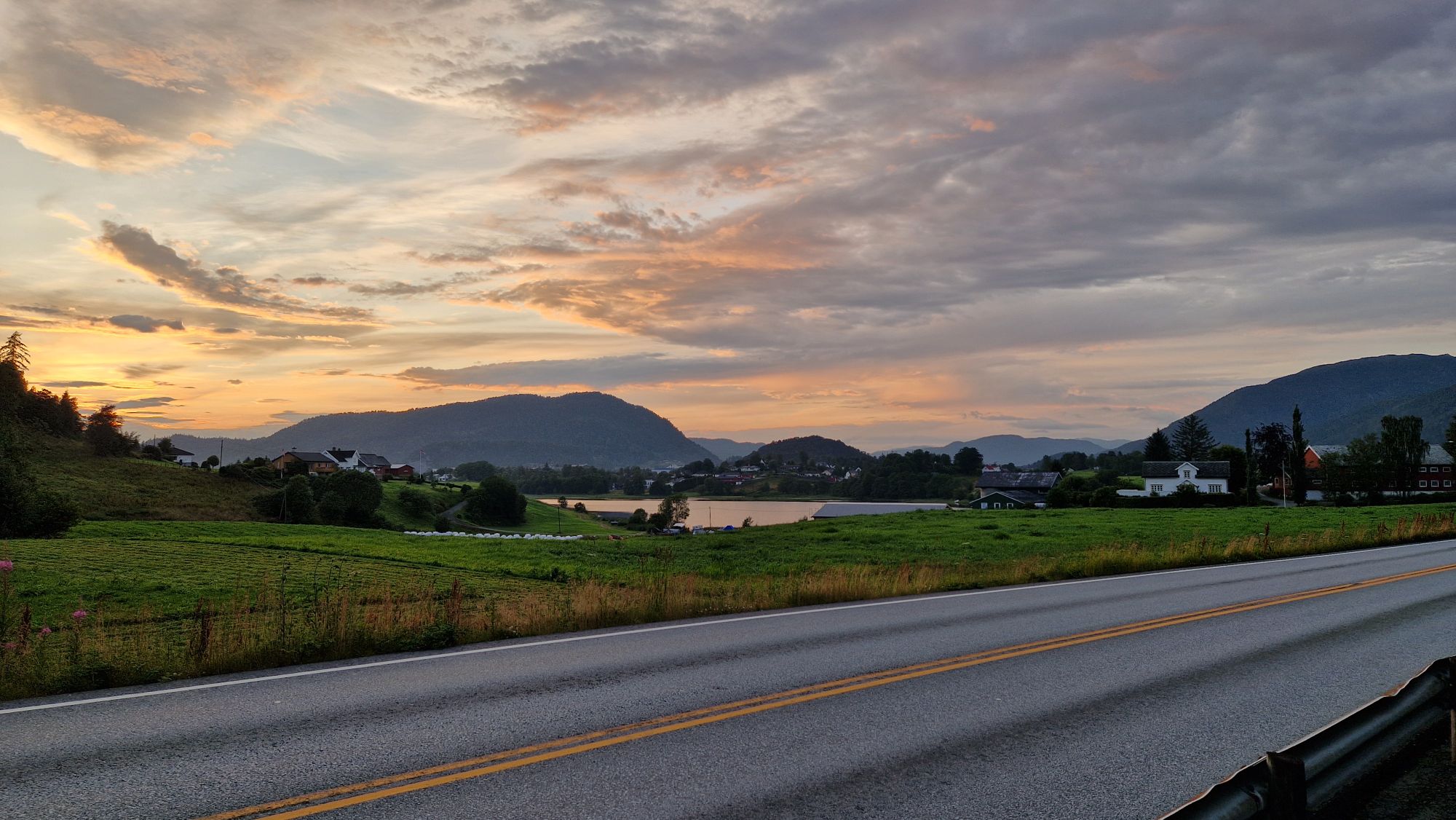
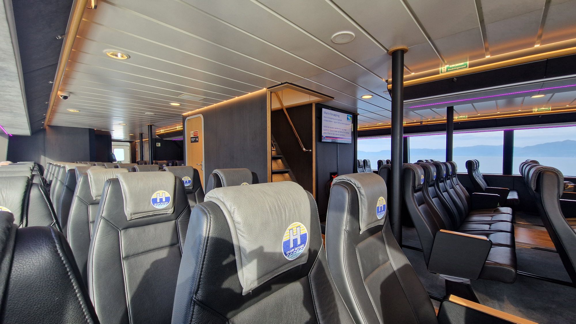
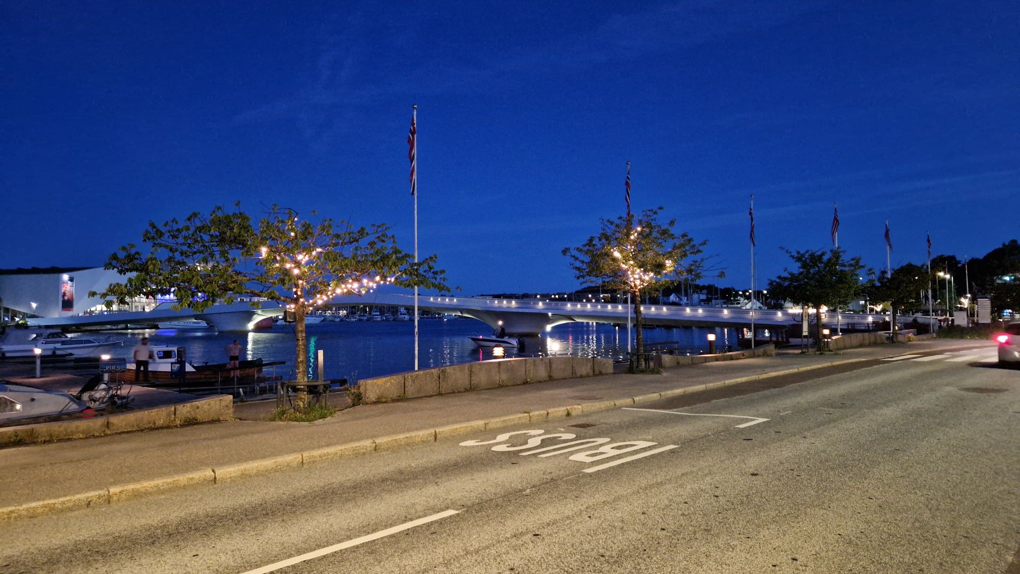
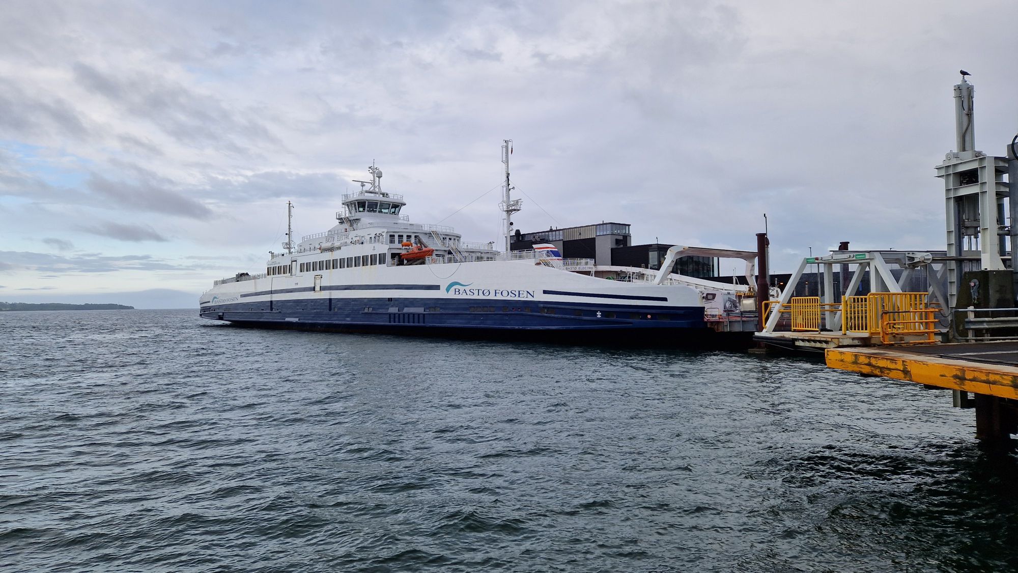
Thursday, July 17th. The travel via Fjordline’s MS Stavangerfjord was very nice. The weather was excellent and the sea was very quiet. The ship itself had everything a traveler could need: shopping centers, restaurants, bars, toilets, cabins of different price classes, a playground, a dog room and perhaps much more. After dinner, I’ve watched the sunset and went sleeping around midnight. At this time of the year far in the north, the sun sets just a bit below the horizon, so we’re always having dusk/dawn and no “full” nights. There were no visible stars except a planet or two.
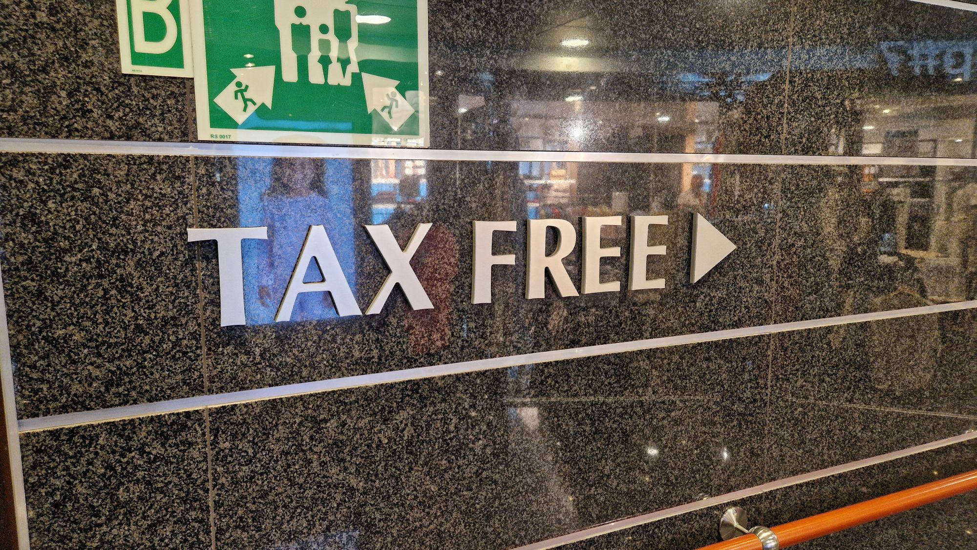
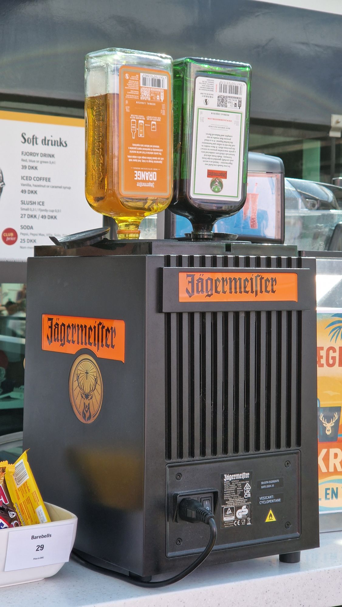
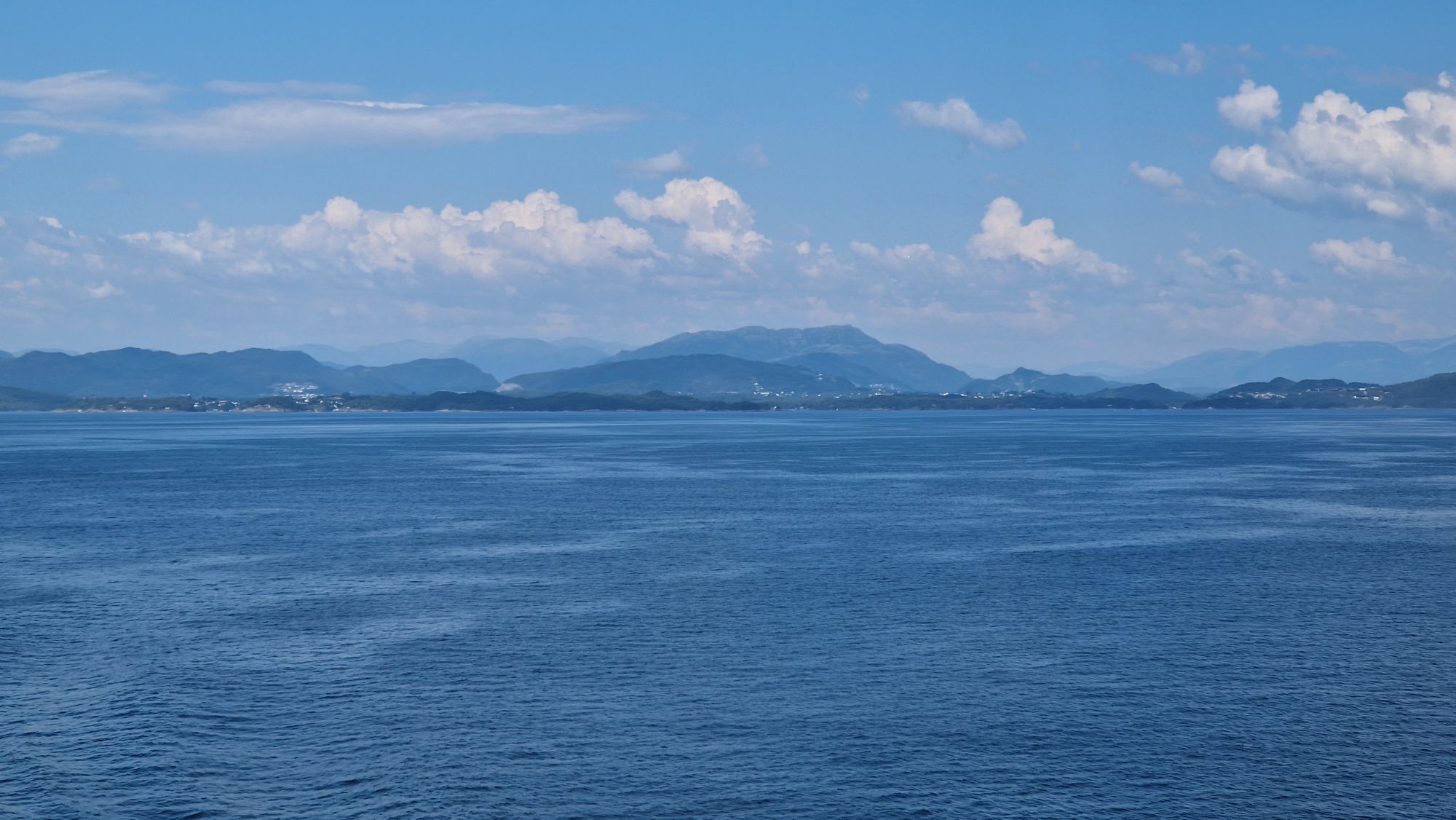
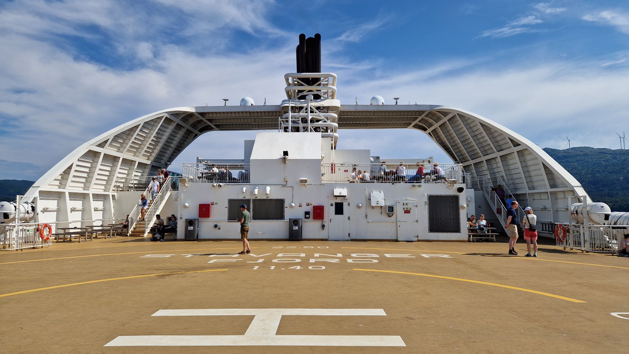
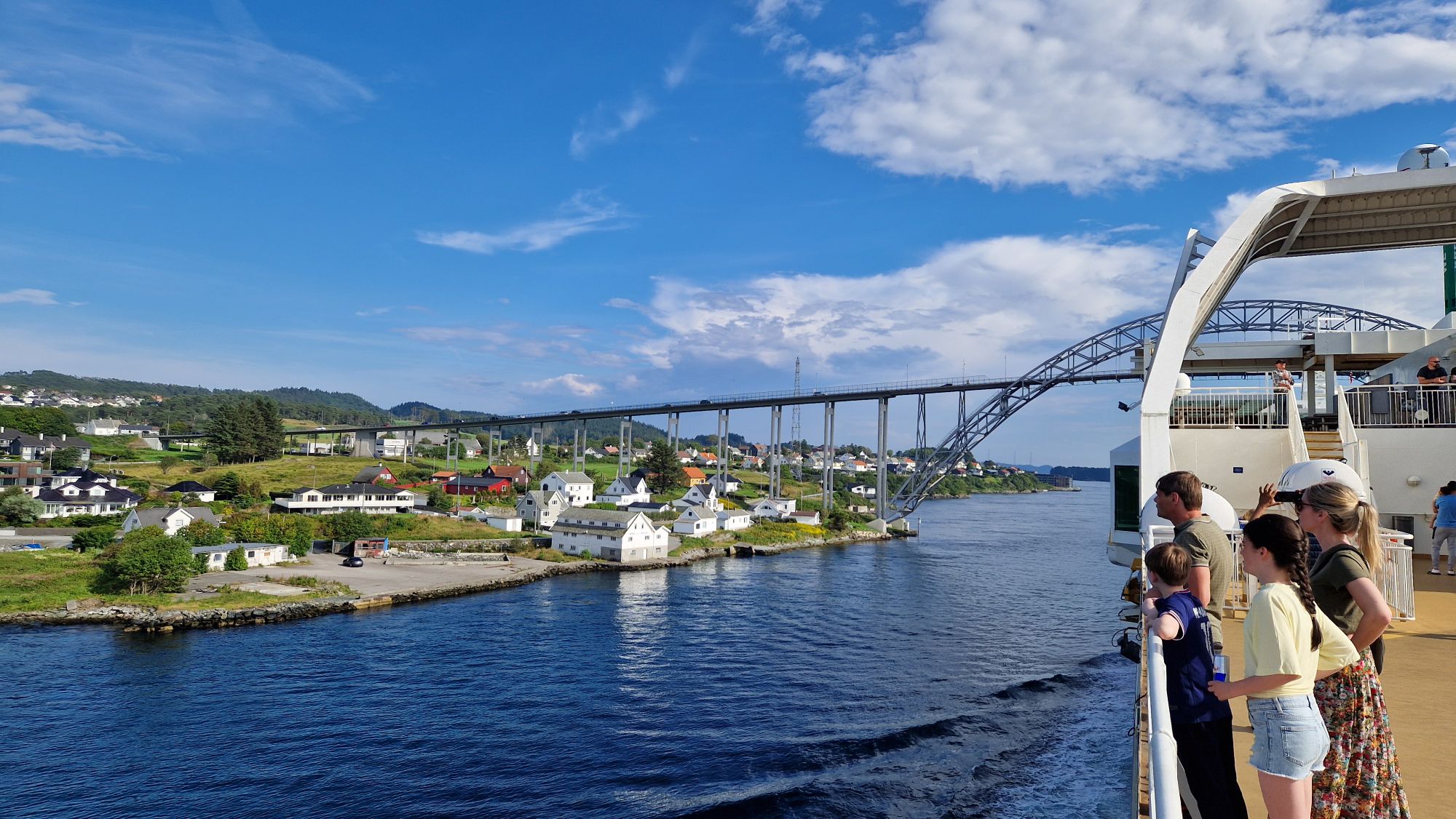
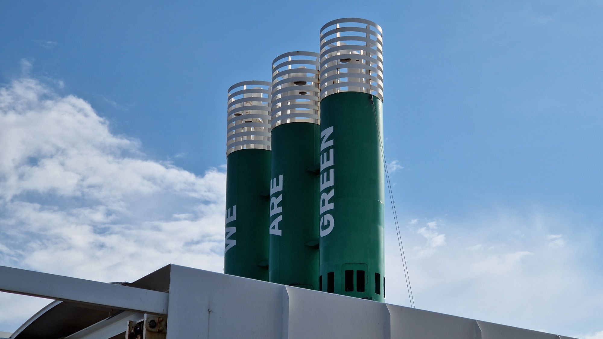
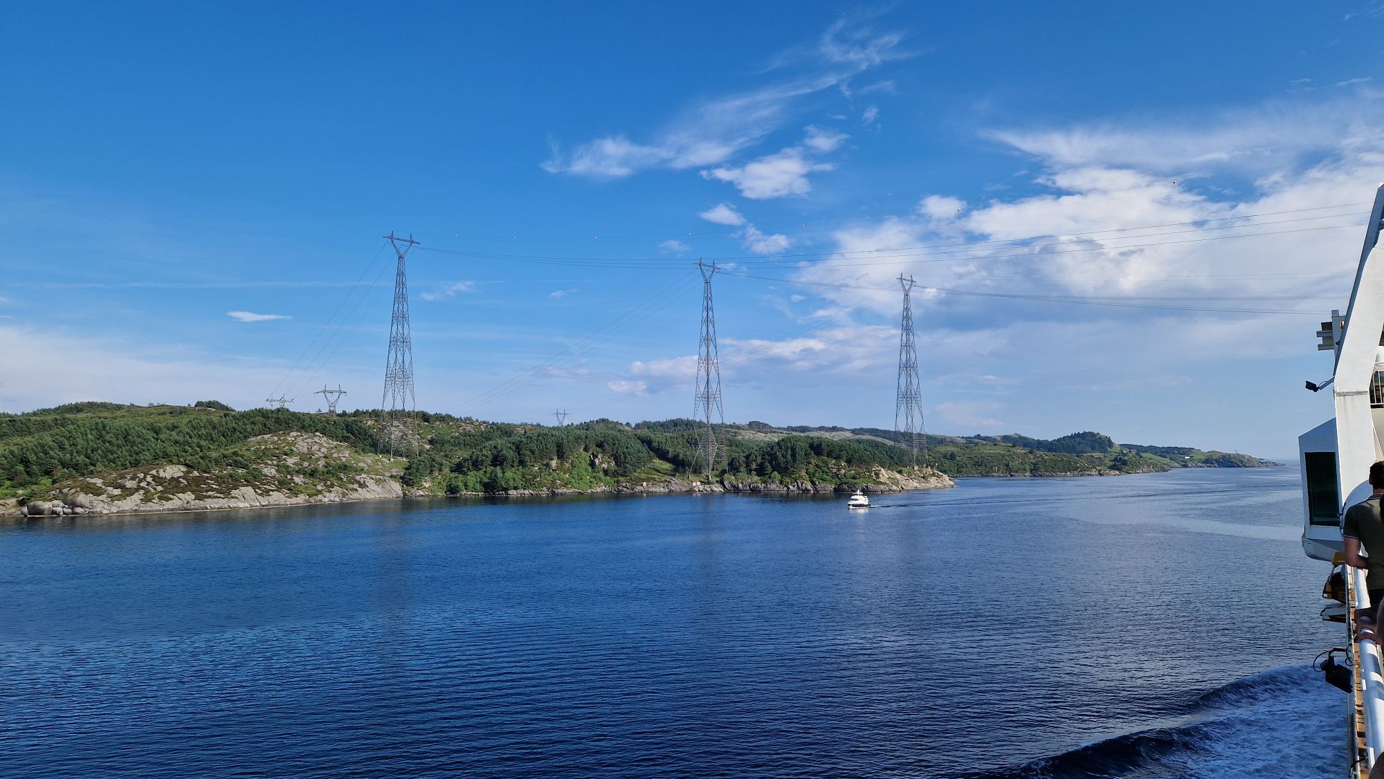
Leaving the Bergen harborTax freedom for 18 hoursInteresting Jägermeister machineViews on the hills, beautiful weatherRear deck of the MS StavangerfjordApproaching a bridge near HaugesundThe power transmission towers near Karmøy, view on FosenGreen painted exhaust chimneysApproaching the Stavanger harbor
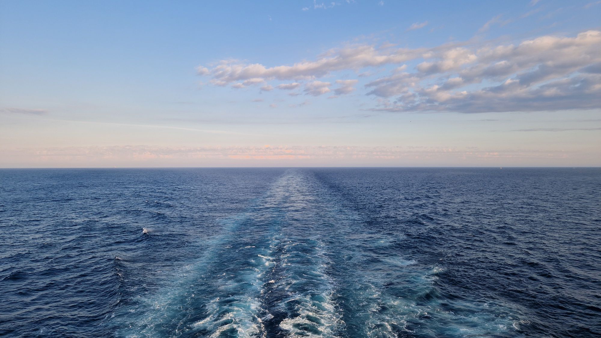
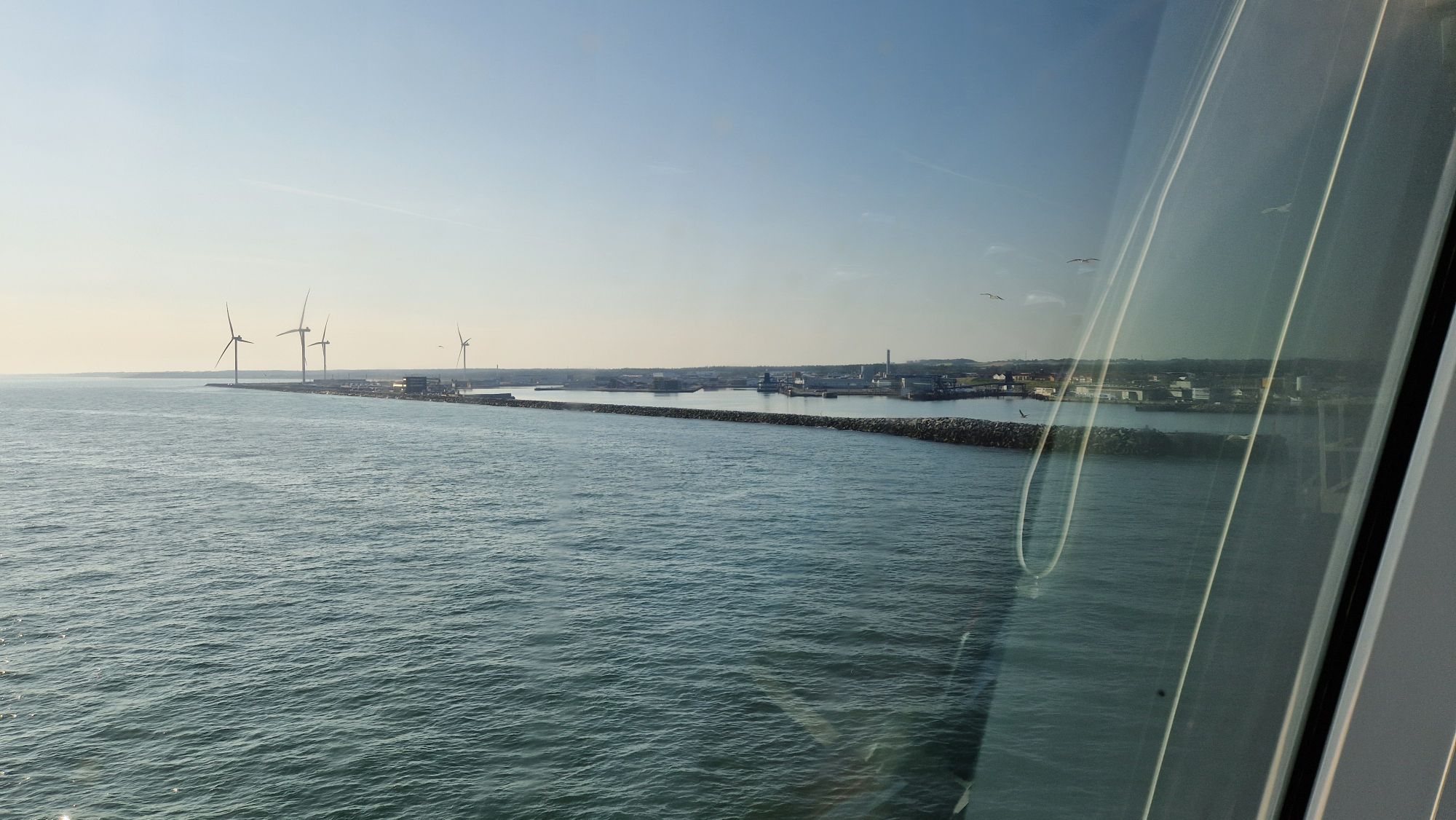
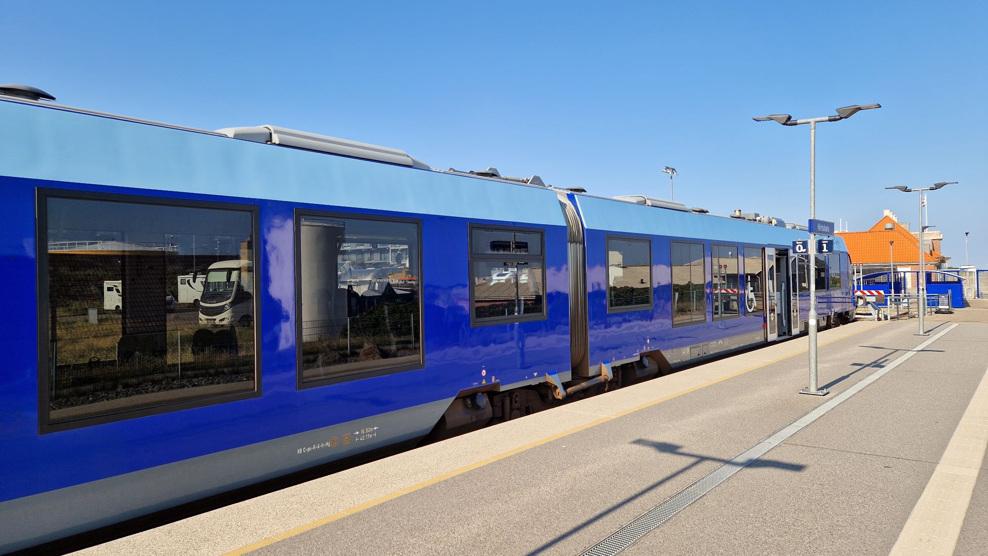
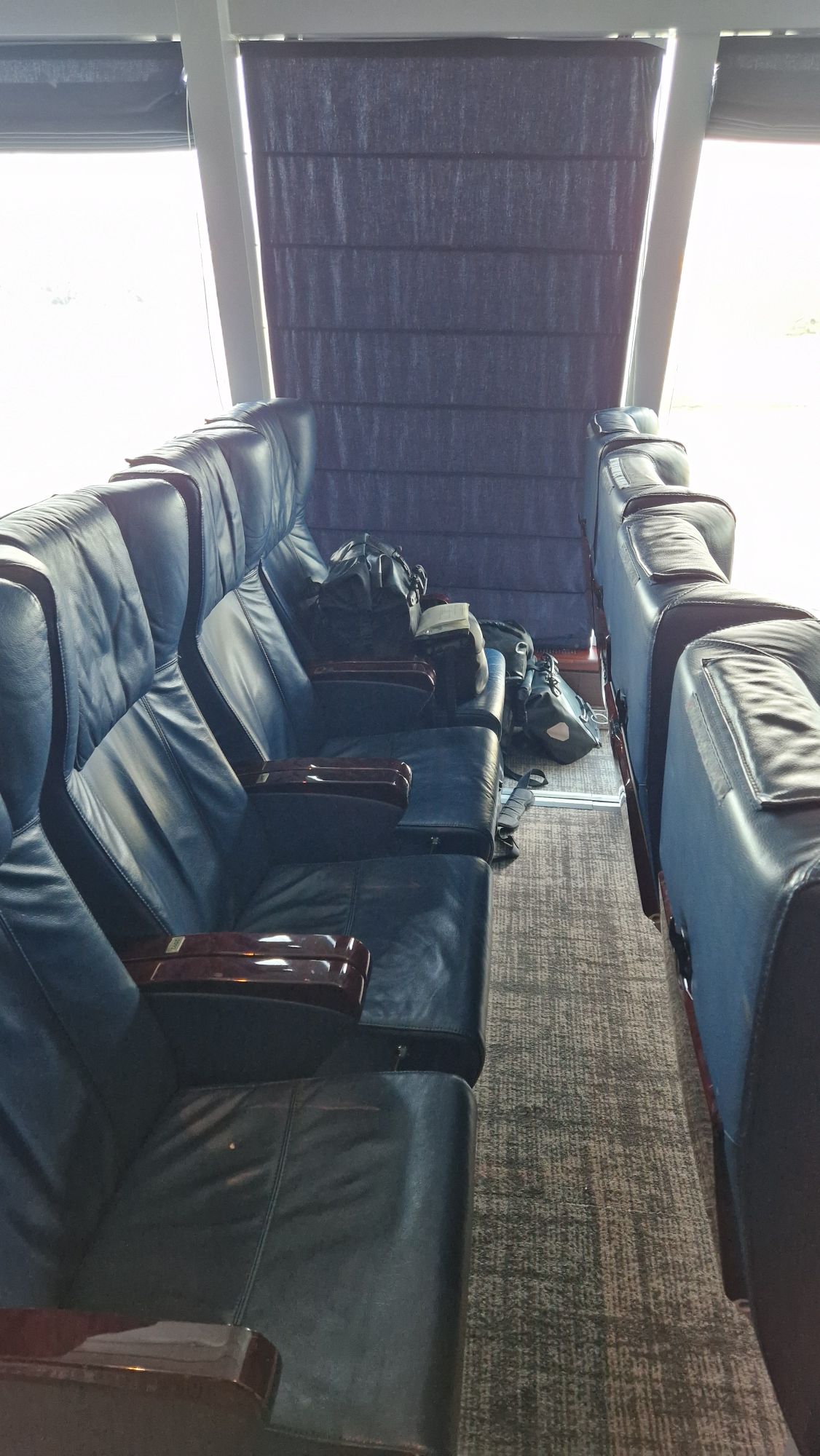
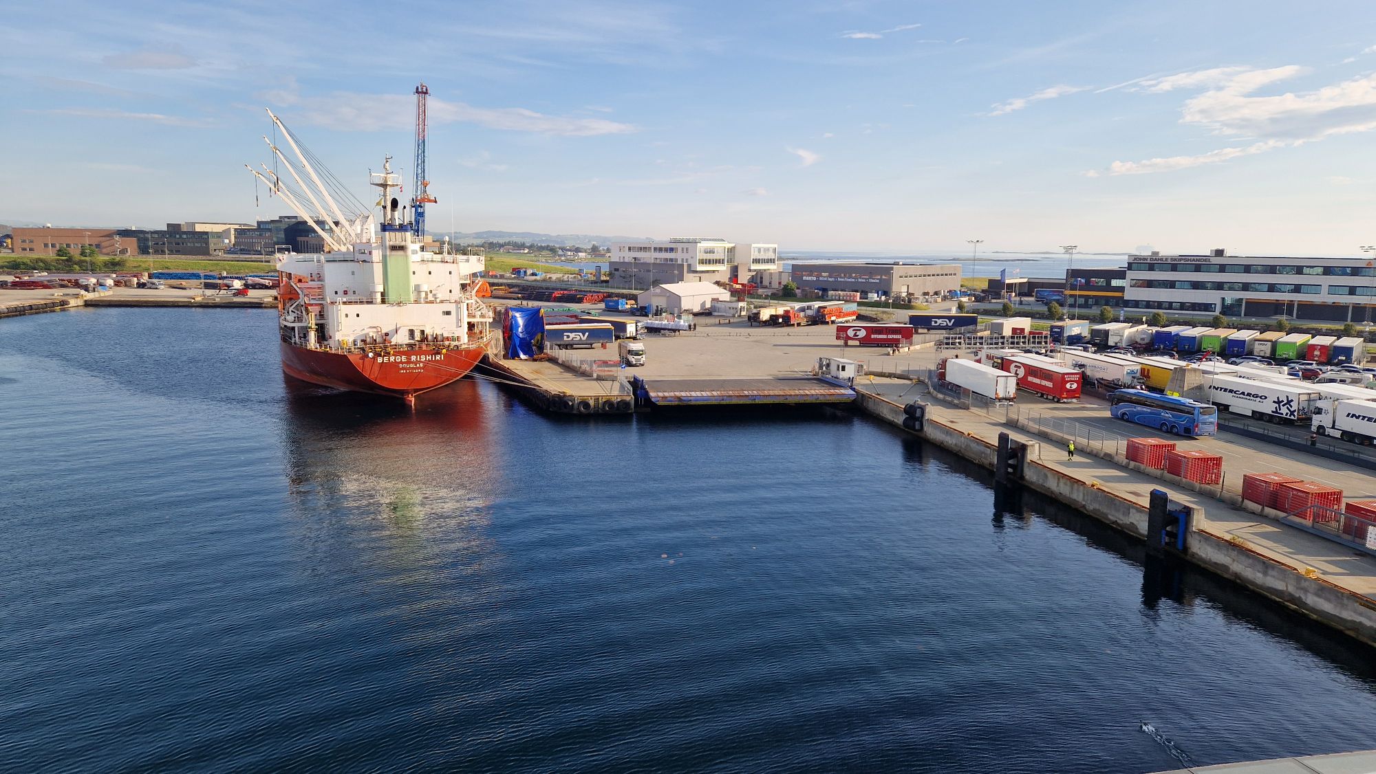
I’ve booked the comfort seat for 31 EUR instead of a cabin for €€€ reasons. Sleeping in such a seat was fine for an hour or so, but I woke up with a hurting neck. Luckily, my room was empty, and I could spread out a bit, which helped me to get a decent amount of sleep. I woke up around 6am and watched the sea a bit before having breakfast and leaving the ship around 8am in Hirtshals, Denmark.
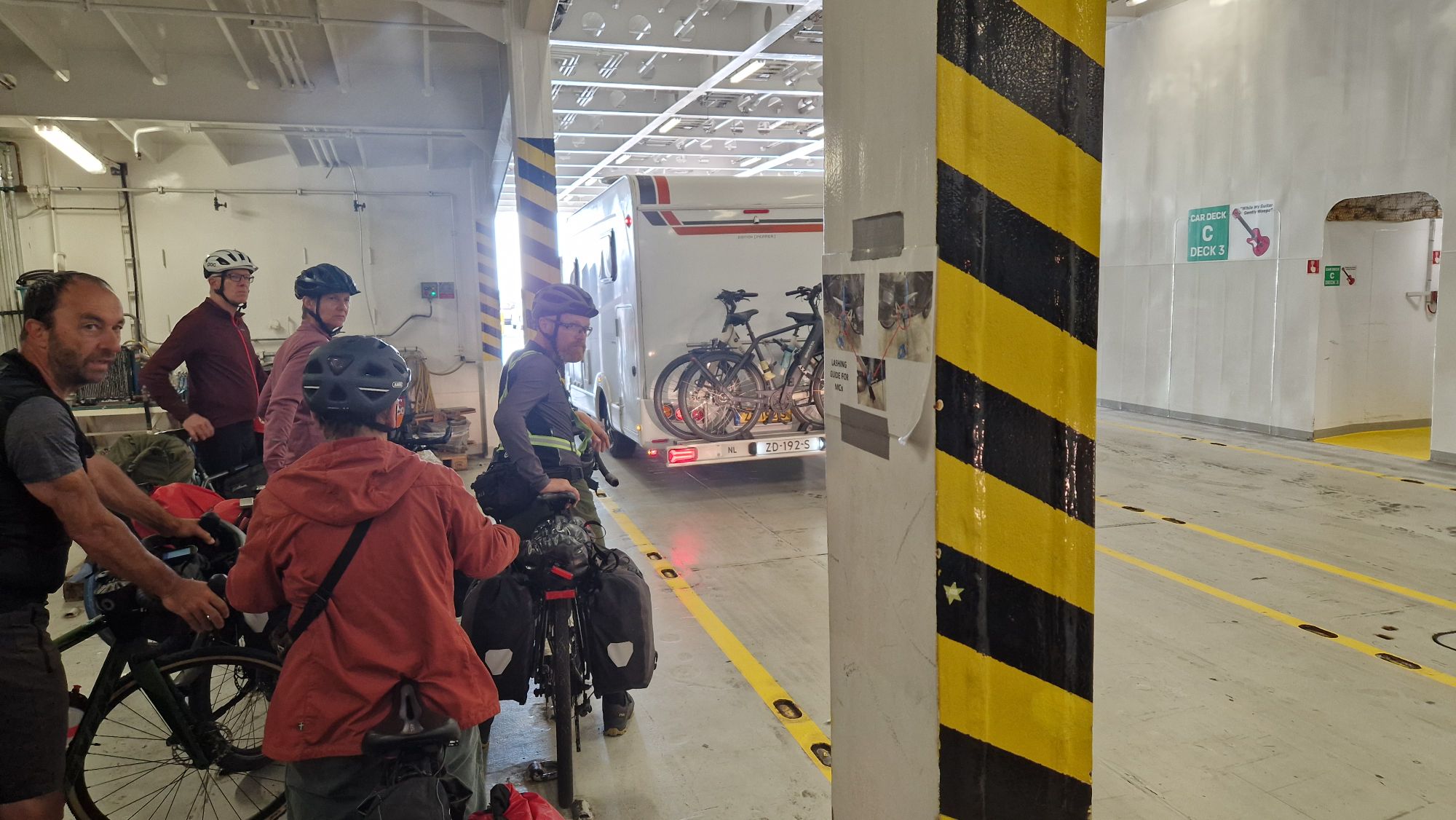
My “dinner”Sea after sunsetSea next morningDanish flag of MS StavangerfjordApproaching Hirtshals harborCyclists getting ready to leave the ship
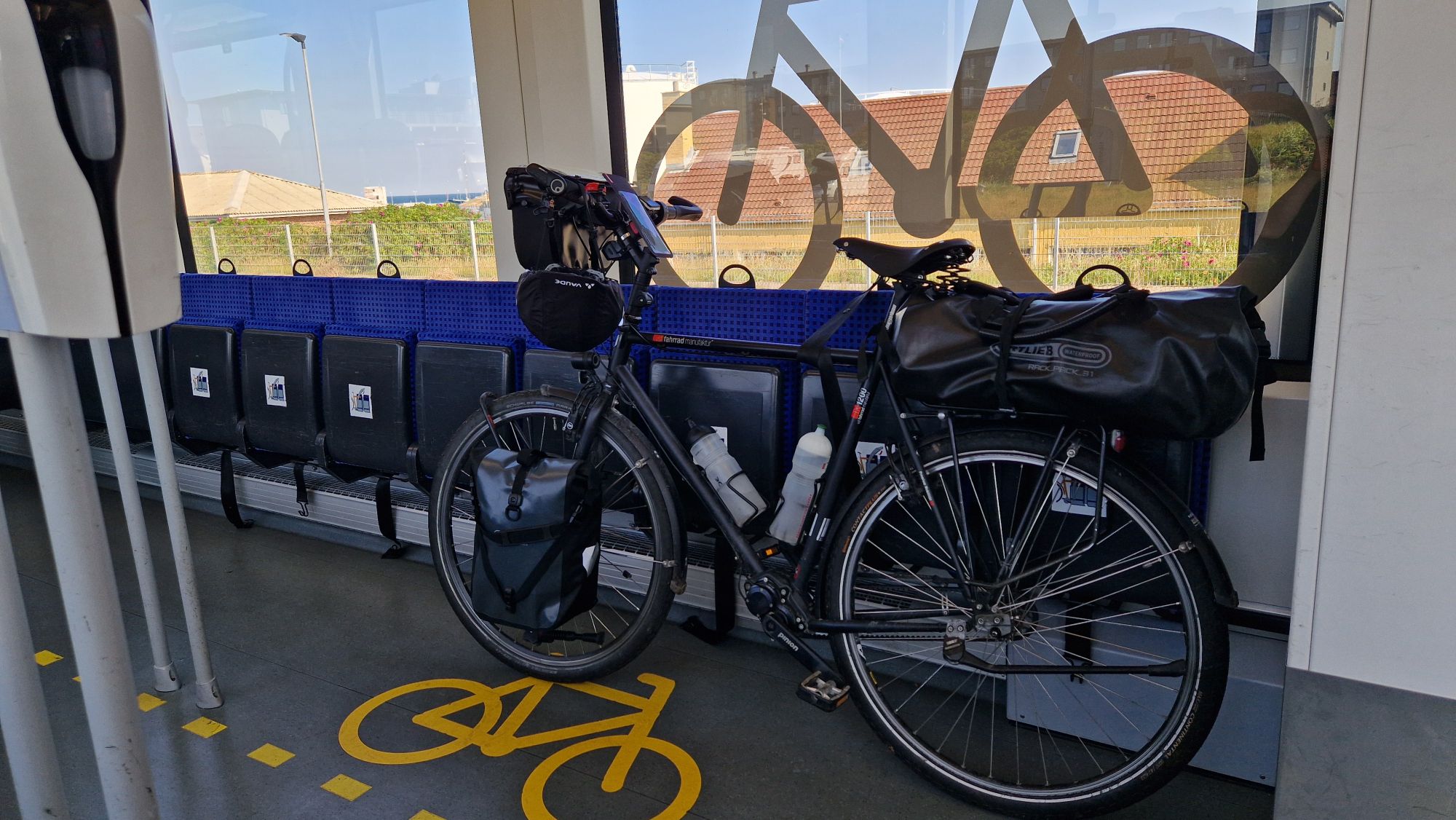
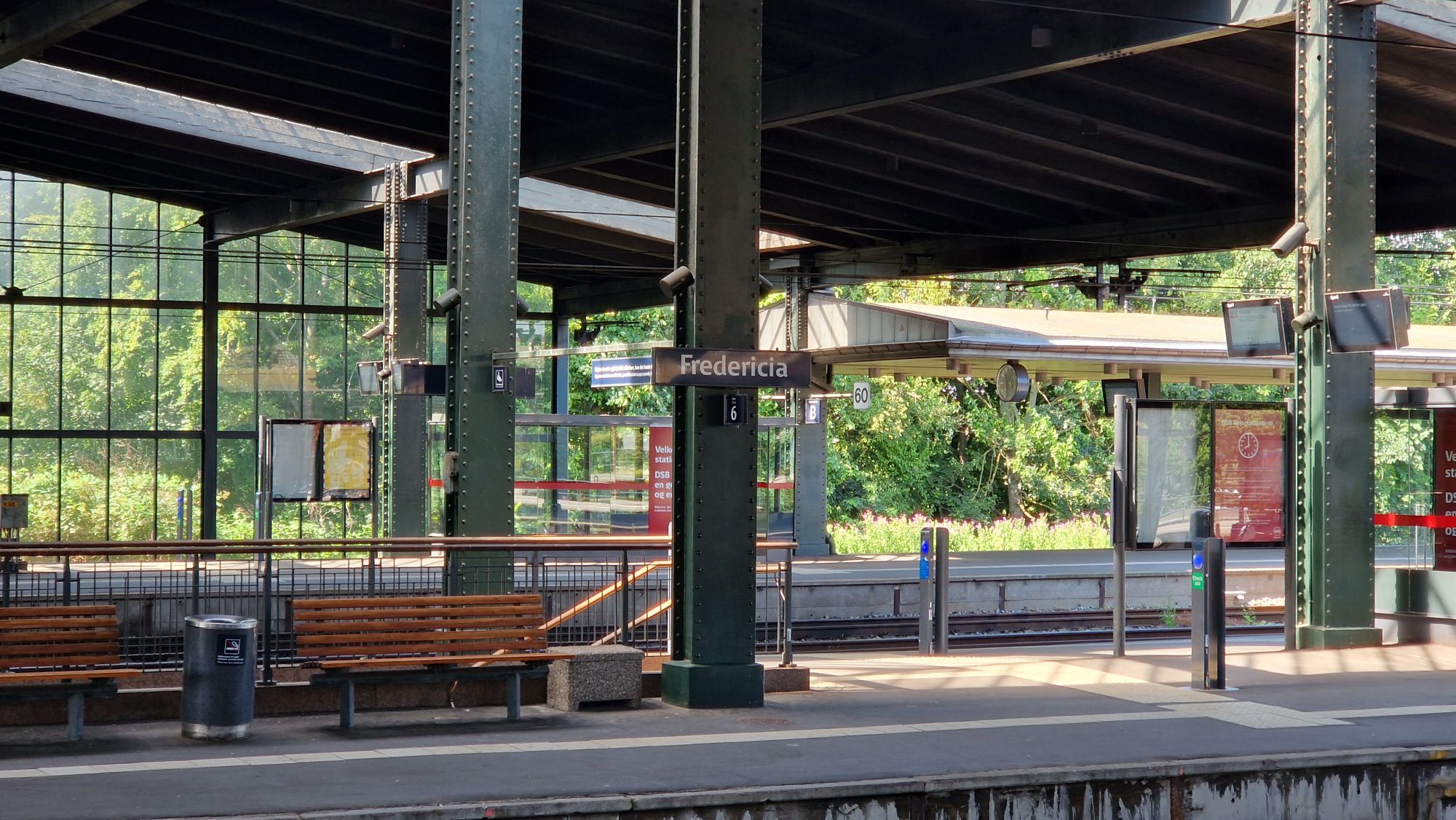
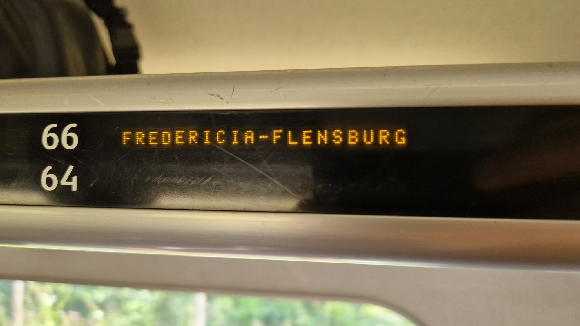
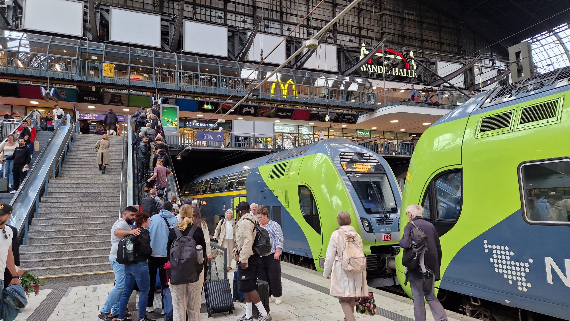
The travel back home continued via trains. I’ve chosen the route Hirtshals – Aalborg – Fredericia – Flensburg, which takes about 6 hours. The price was 416 DKK, which is about 56 EUR. Flensburg – Braunschweig takes another 6.5 hours by regional trains if the trains are on time (price around 50 EUR + 7 EUR for bike ticket). I’ve had some time to finish my blog entries while passing all the places from the Denmark 2025 Tour. It really felt like speedrunning Denmark. All Danish trains were on time and the train personnel was very friendly. The bicycle compartments were a little bit full with cyclist’s bikes and families with strollers. We managed the remaining space very well. I started in Hirtshals at 9:42am and arrived in Flensburg at 3:52pm.
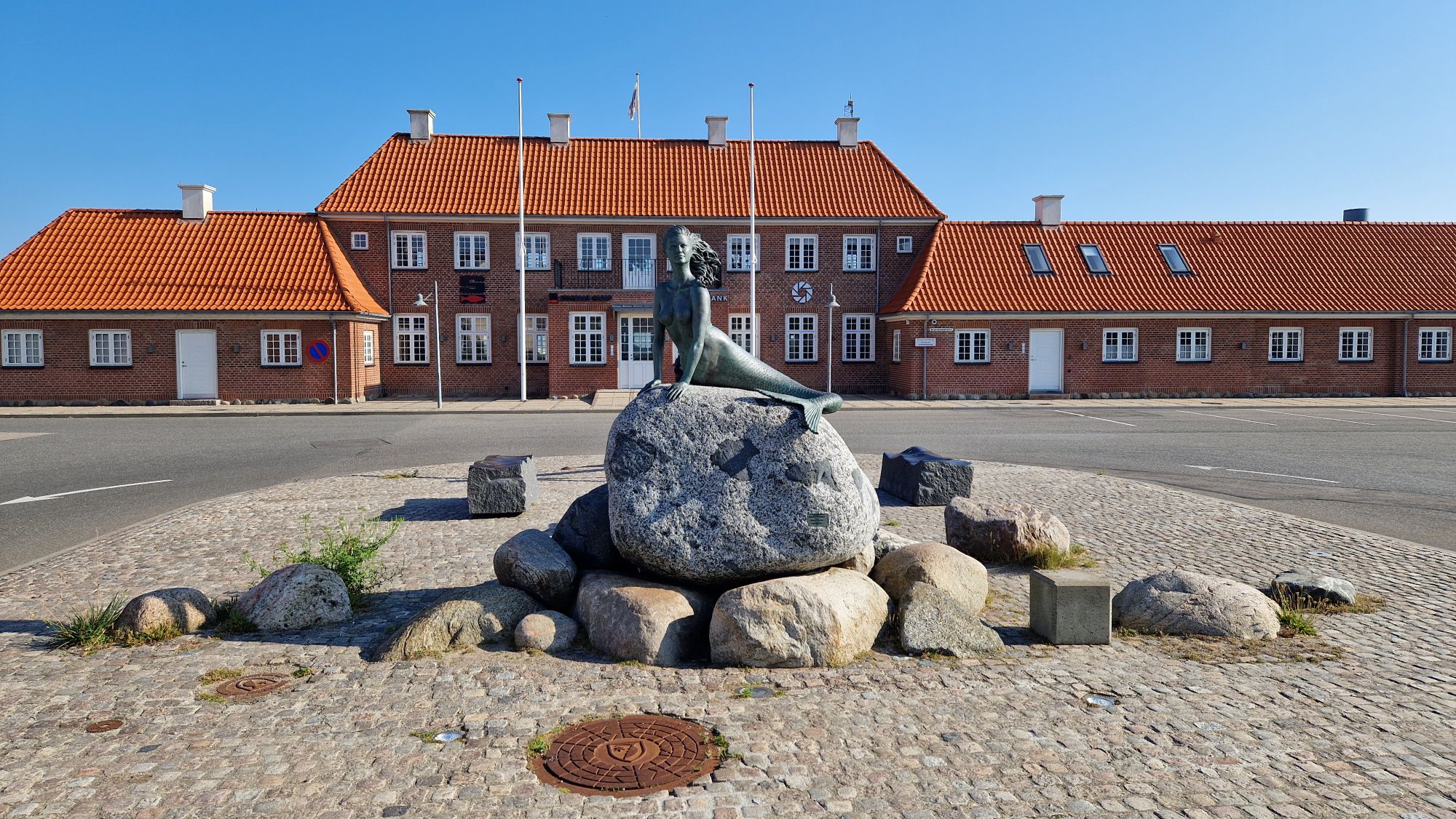
Naked mermaids all over HirtshalsTrain from Hirtshals to AalborgSecured bike in the trainShort train change at Fredericia stationThe travel goes on to FlensburgFew hours later at Hamburg central station
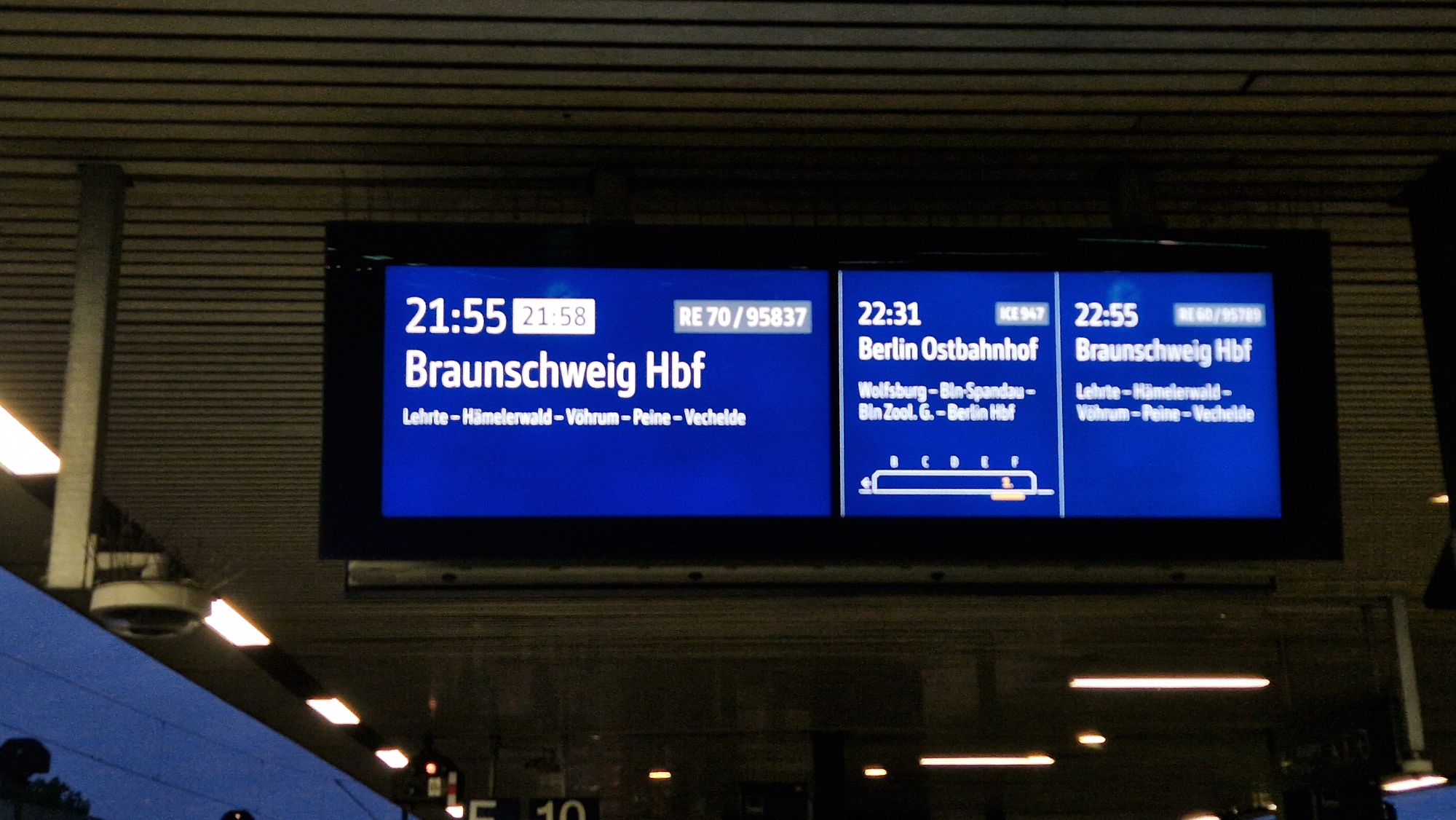
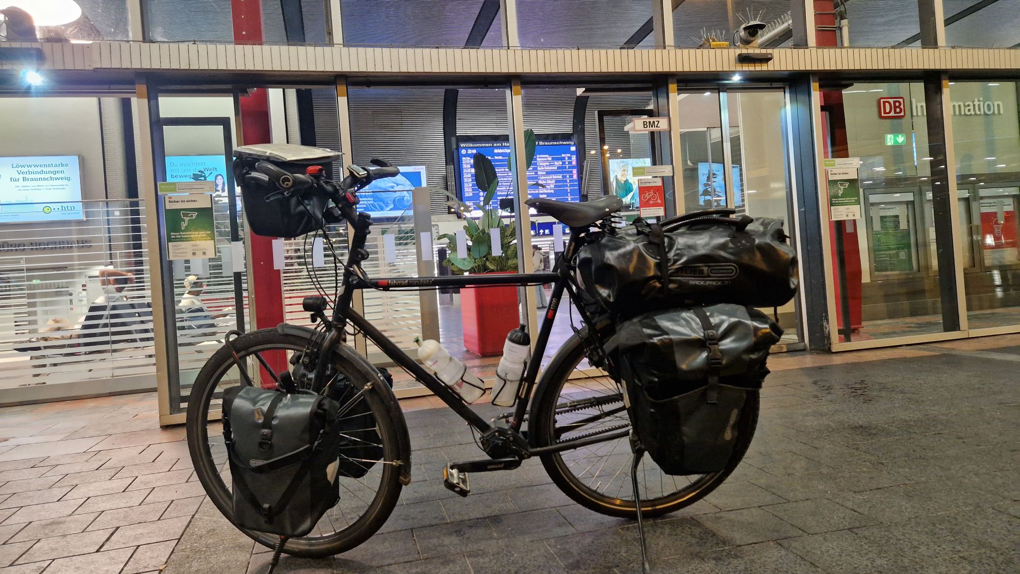
The remaining route from Flensburg to Braunschweig via Hamburg, Uelzen and Hannover was fine with few minor inconveniences. I arrived in Braunschweig at 10:40pm and cycled a bit back home in bad weather and heavy rain.
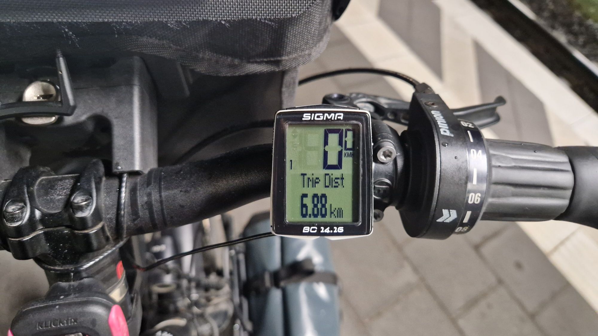
Last train change of the day, Hannover to BraunschweigCycling distance from Hirtshals to Braunschweig: only ~7 km!Finally arrived in BraunschweigWeather in Braunschweig at my arrival. Rain
So there you have it: I traveled back home from Bergen back to Braunschweig in only 33 hours (18h by ferry, 15h by trains). The total price was around 350 EUR. The price and travel time can vary, depending on various factors.
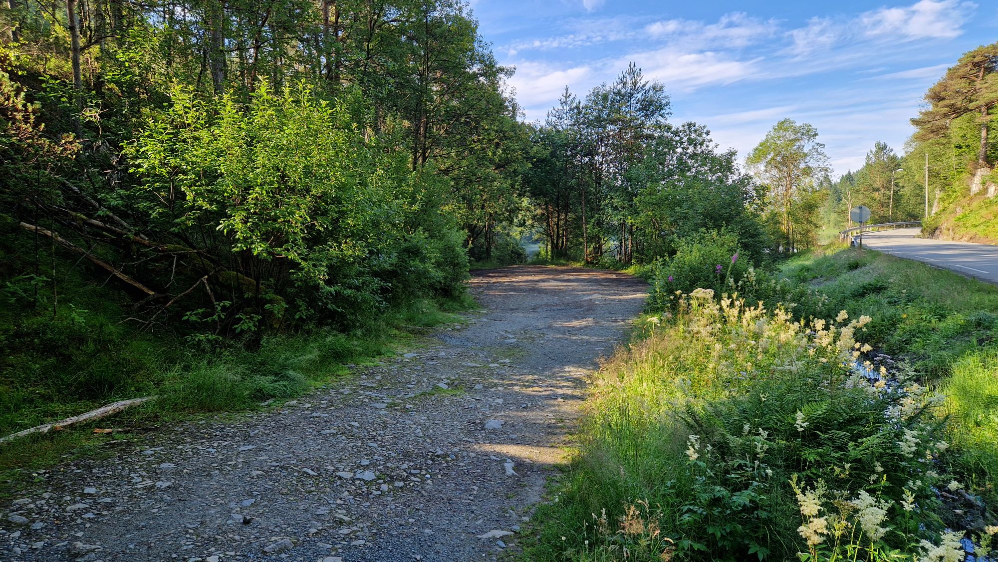
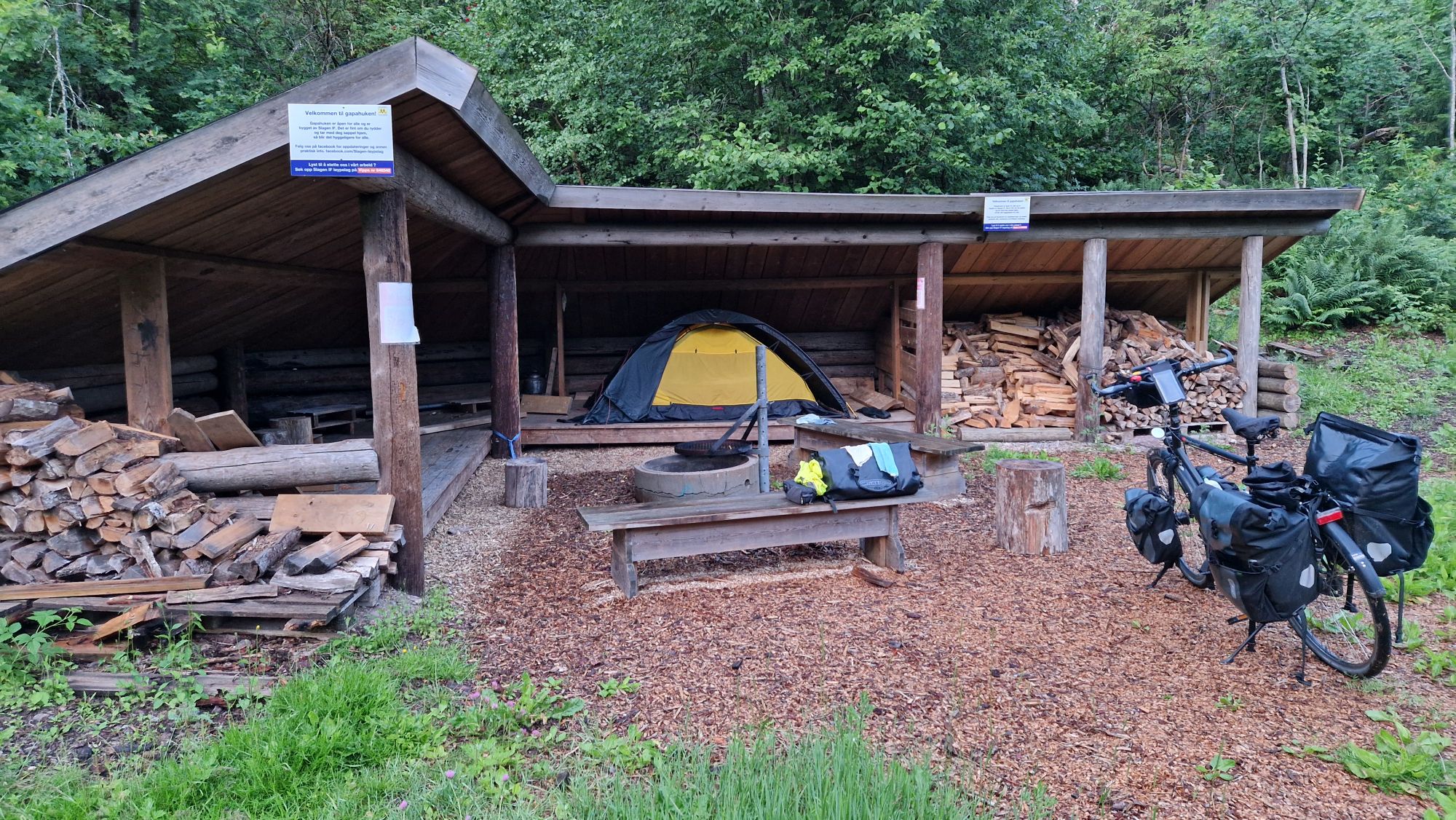
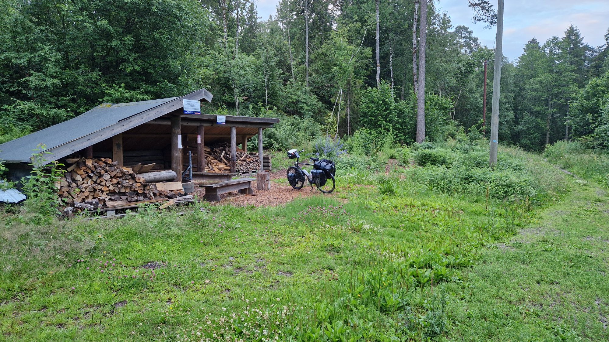
Wednesday, July 16th. I slept fine at the shelter and woke up around 8:20am. I checked the ferry schedule again and the departure was at 2pm, some 5.5h away. After checking the navigation again, this seemed possible. I thought about ~3 hours of riding the bike to Bergen and according to Fjordline, the check-in would take 1 hour prior to departure.
So, around 8:30am, I started packing my stuff and omitted unnecessary tasks. About 45 minutes later, I was on the road to Bergen. A few hills awaited until a really big and steep hill made me push the bike for 30 minutes. I’ve climbed 180 meters and was sweating so much that my clothes felt like I came back from swimming. After reaching the top, the descent was followed fast and steep roads with many curves which killed my speed. Despite my worn-out brake pads and screaming braking, everything went well and I liked the fast descent a lot (to cool down and dry my wet clothes).
Shelter on next morningViews on the nearby lakeGravel road to the shelterIt’s getting steep hereAt the top of the hillLocation of the peak, ready to descend
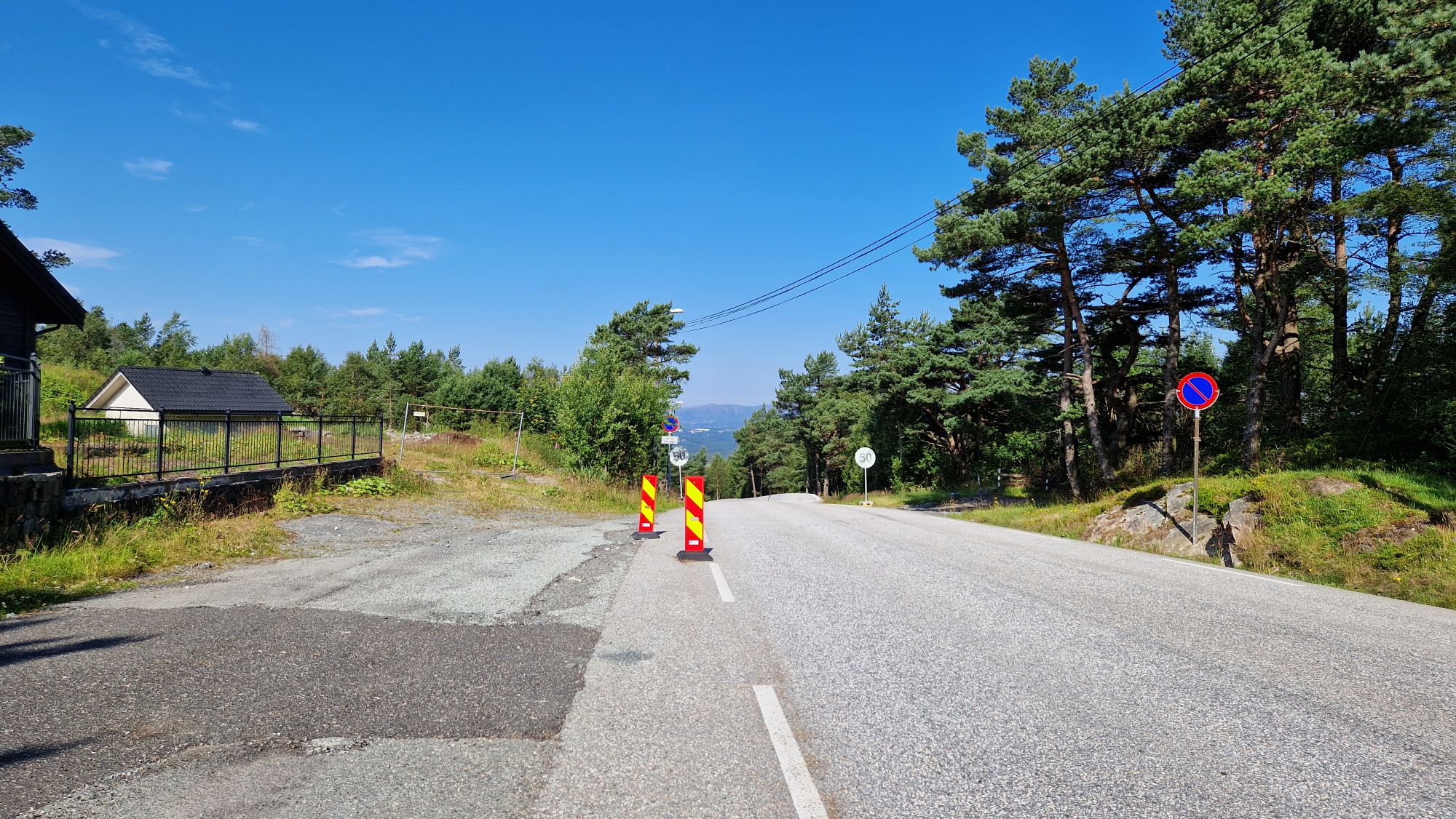
Luckily, that hill was the only bigger obstacle on route, and the remaining 17 km to Bergen were mostly flat and easy to ride. However, there were a bunch of closed cycling roads due to construction sites, which were annoying when riding under time pressure.
Some 3 km away from Bergen Sentrum, I ordered my ticket for the ferry from Bergen to Hirtshals (Denmark) via Stavanger. The ticket cost me 143 EUR plus some additional 100 EUR for a dinner, breakfast and a “relaxing chair” (basically a comfortable sleeping armchair). I did not book a cabin. Otherwise, the costs would have doubled easily.
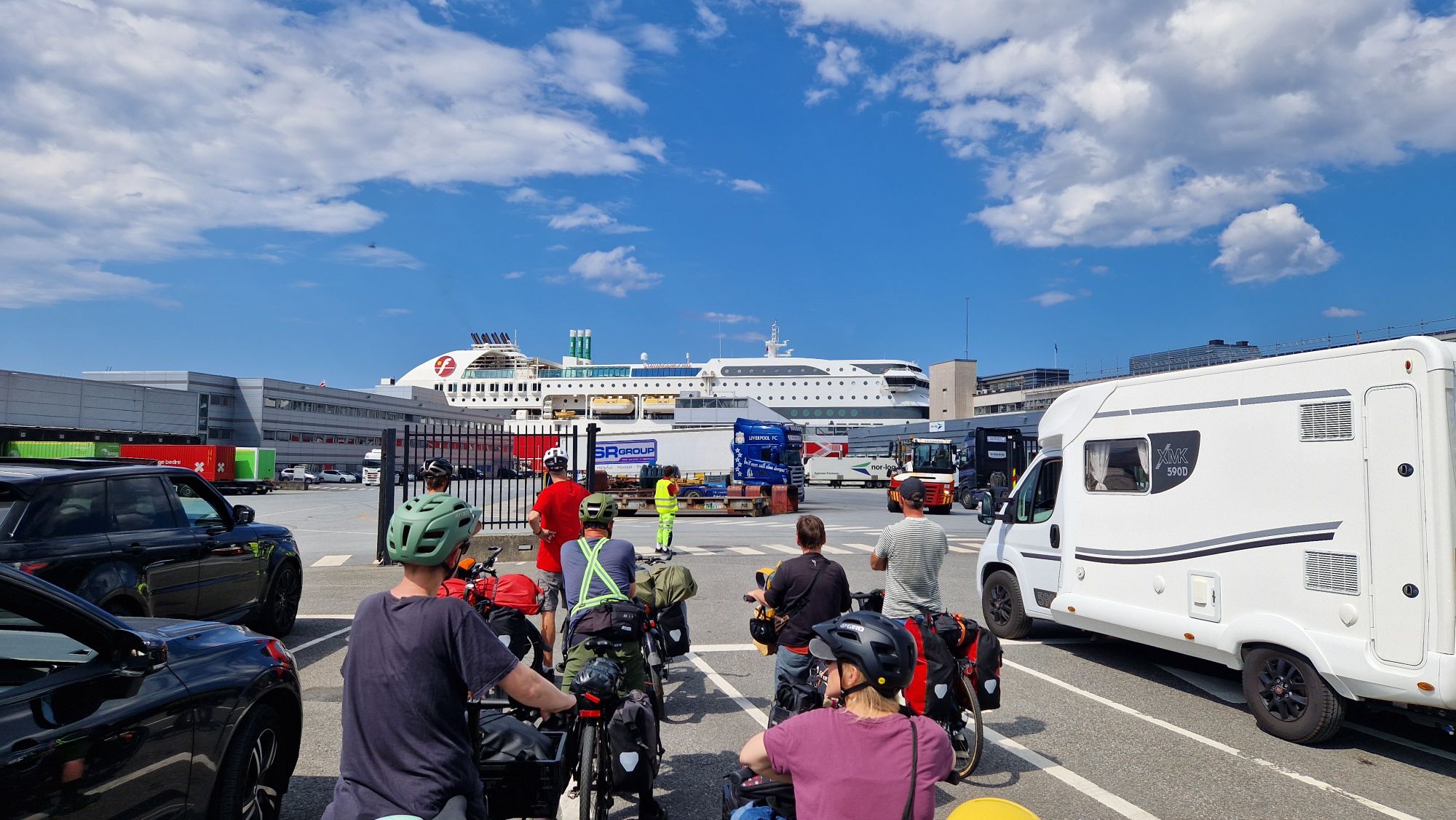
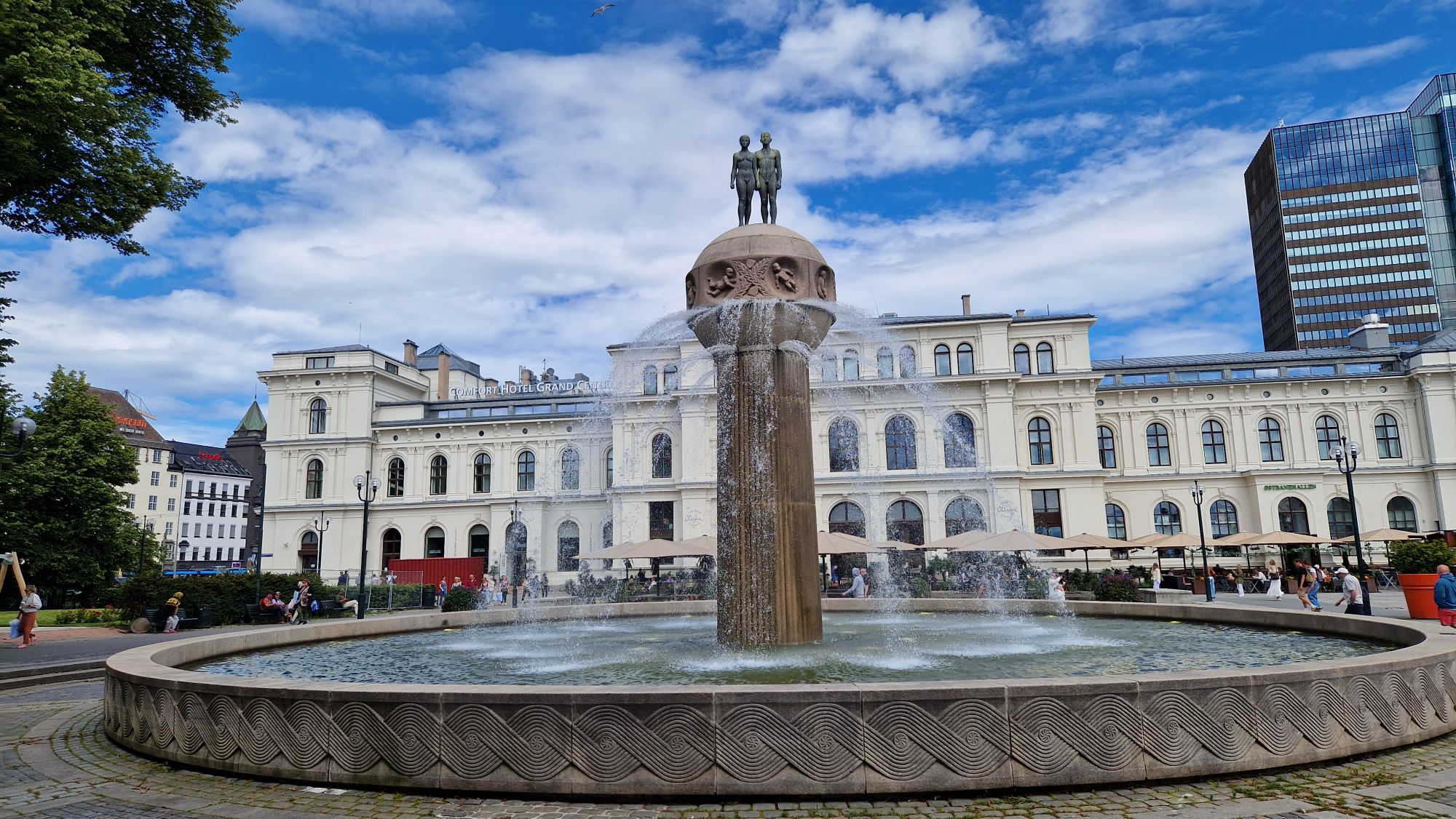
View on a hillMemes and artSelfie on a bikeColorful housesNice buildingTook a small break at this park fountainNaked people all over the placesNaked guy all over the placesNaked seagullCyclists ready for boardingI’ve cycled from Malmö to Bergen in 22 days, a total distance of 2120 km
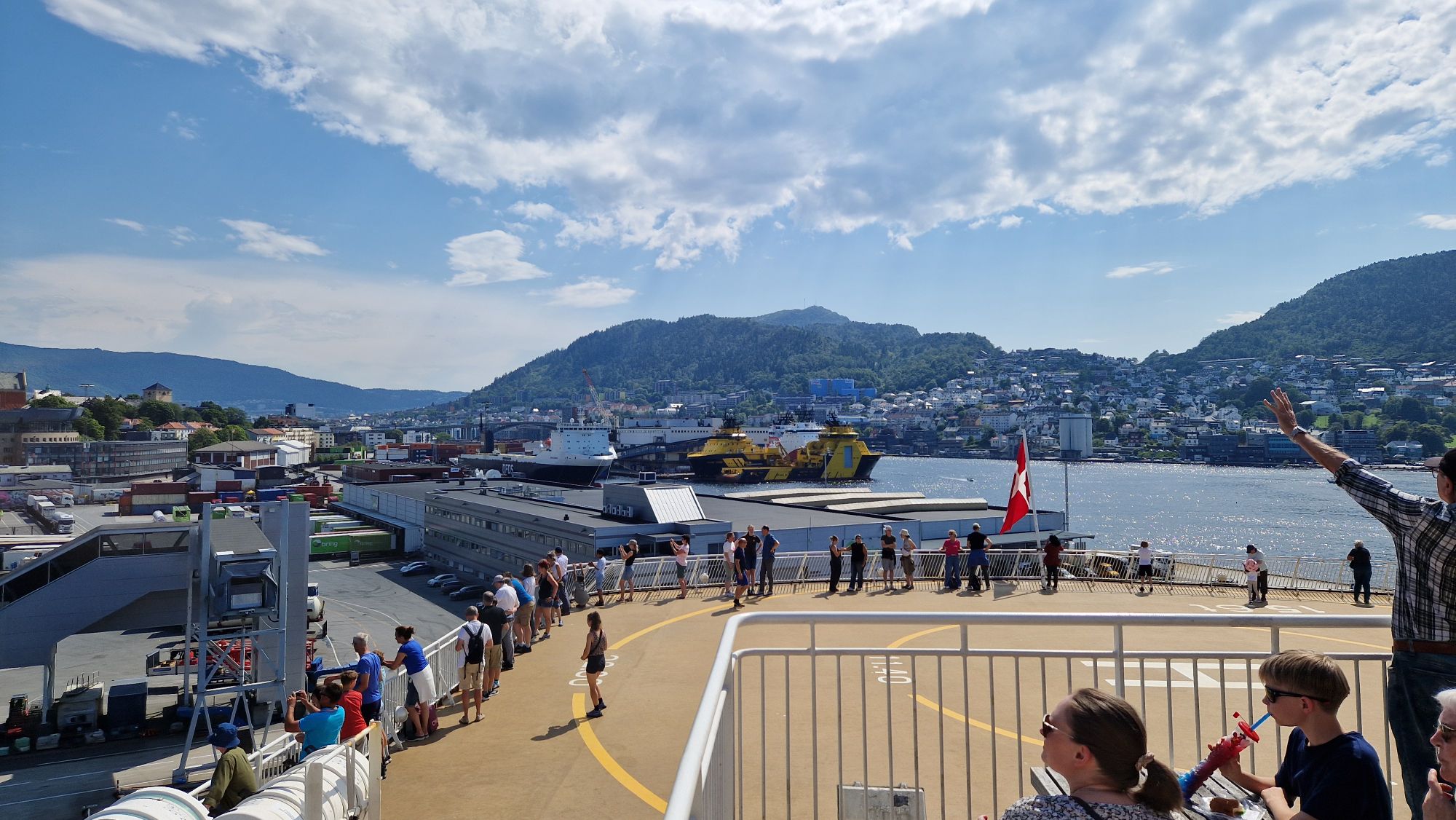
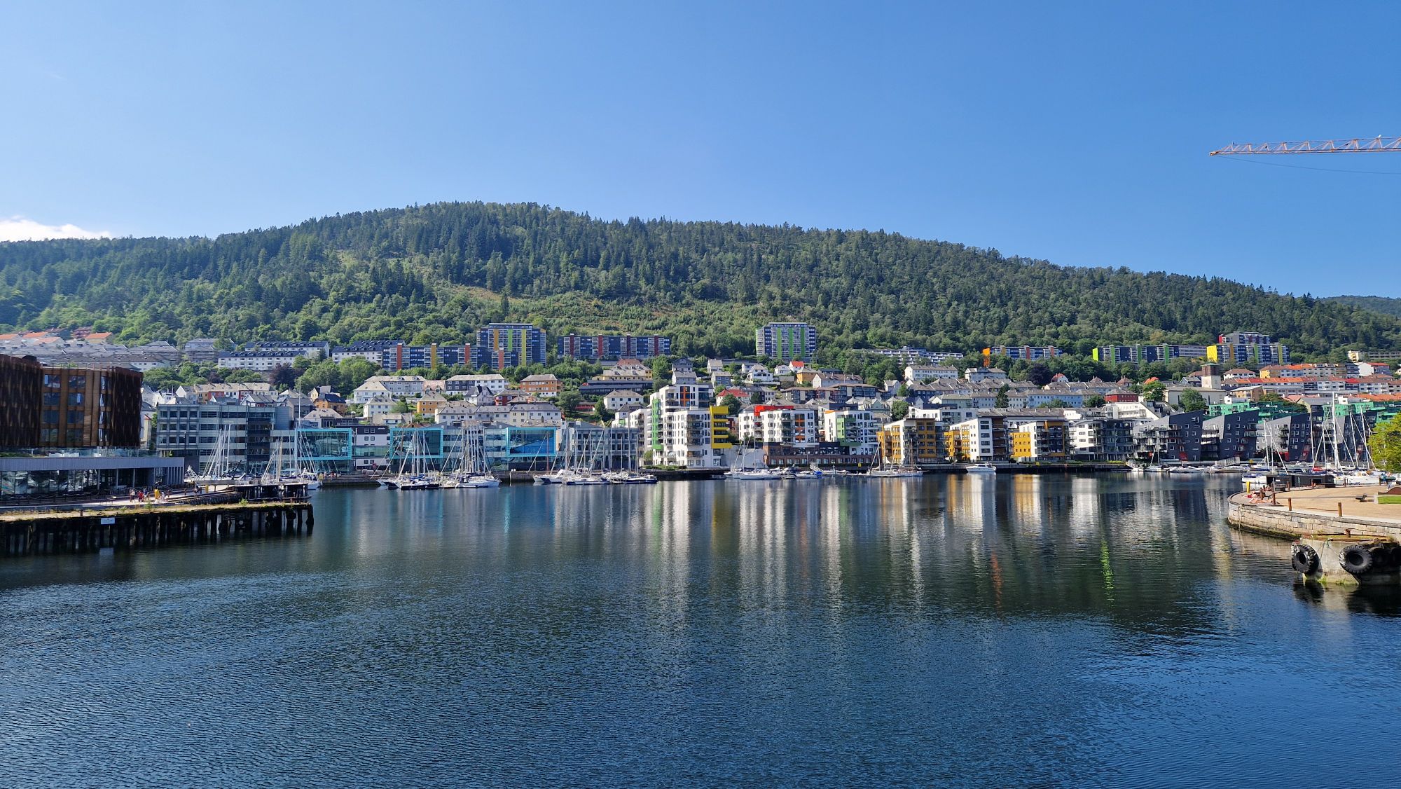
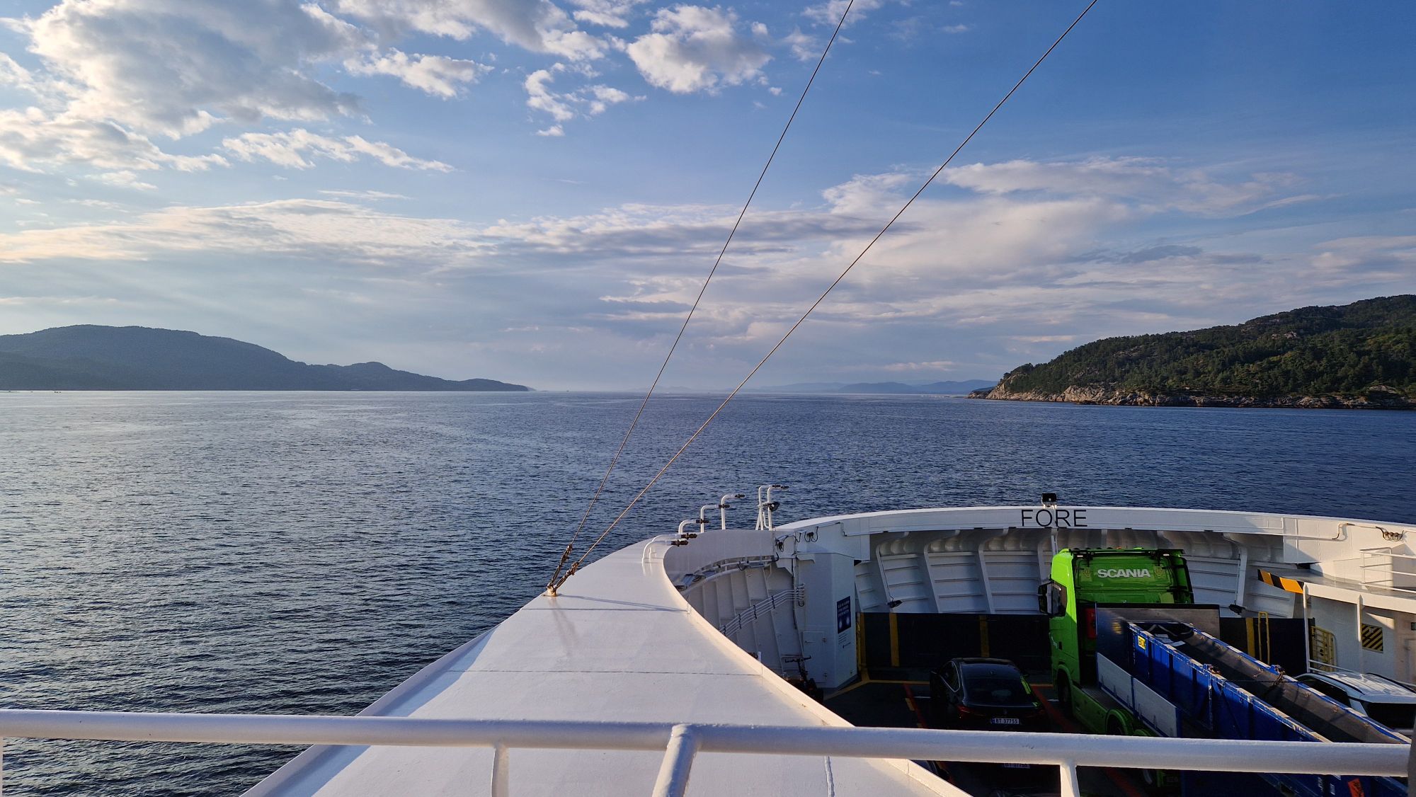
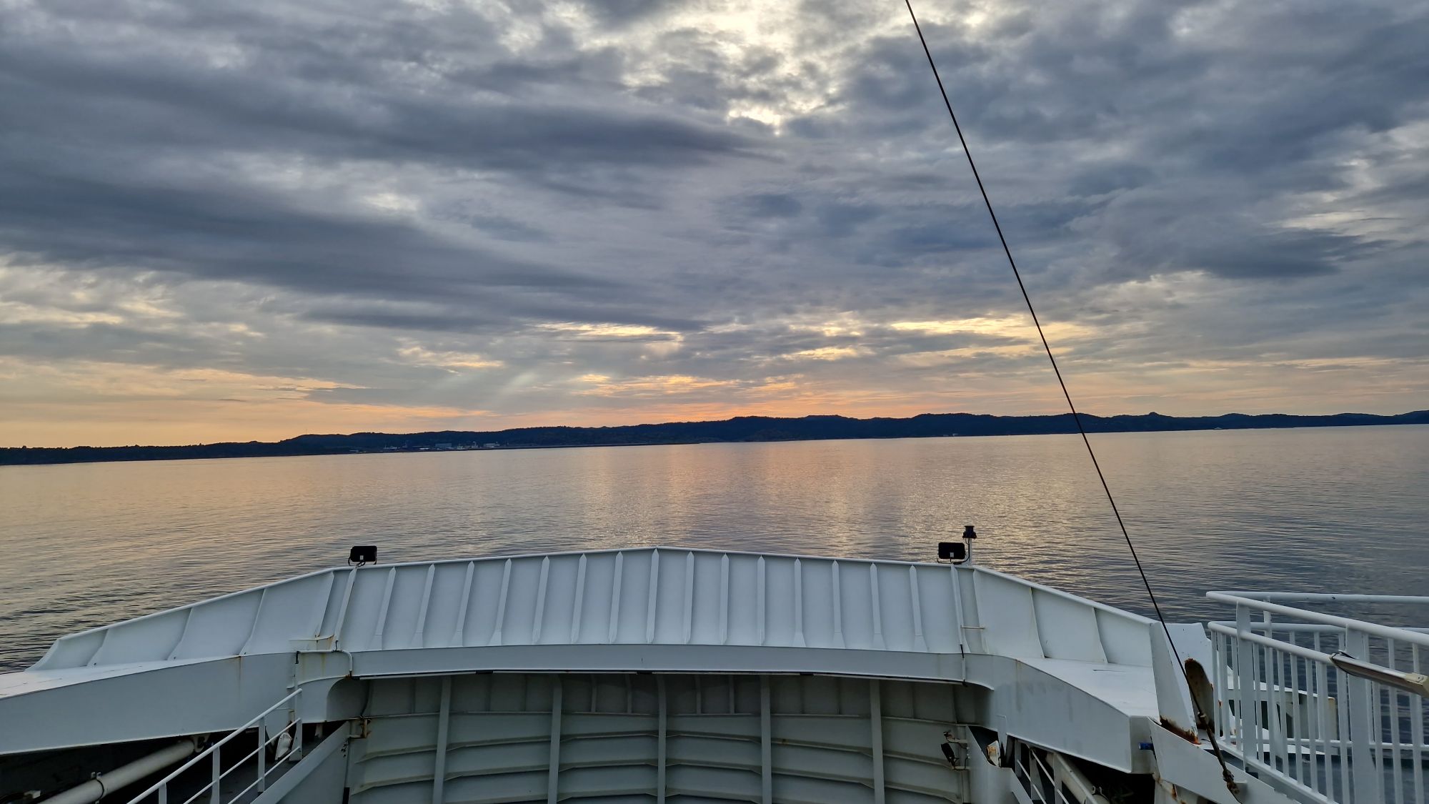
So I arrived in Bergen central at noon, made some photos along the way but didn’t see very much. I will close this educational gap next year. The boarding process was fairly easy – the crew guided us to the lowest deck where we would park and secure our bikes. After doing so, I went to the top deck just as we started leaving the harbor. I literally made hundreds of photos and enjoyed this departure very much. I spent the whole afternoon and evening on top deck taking photos and staring at the Norwegian coastline, the passing ships, the blue sky – and later – the amazing sunset on the sea.
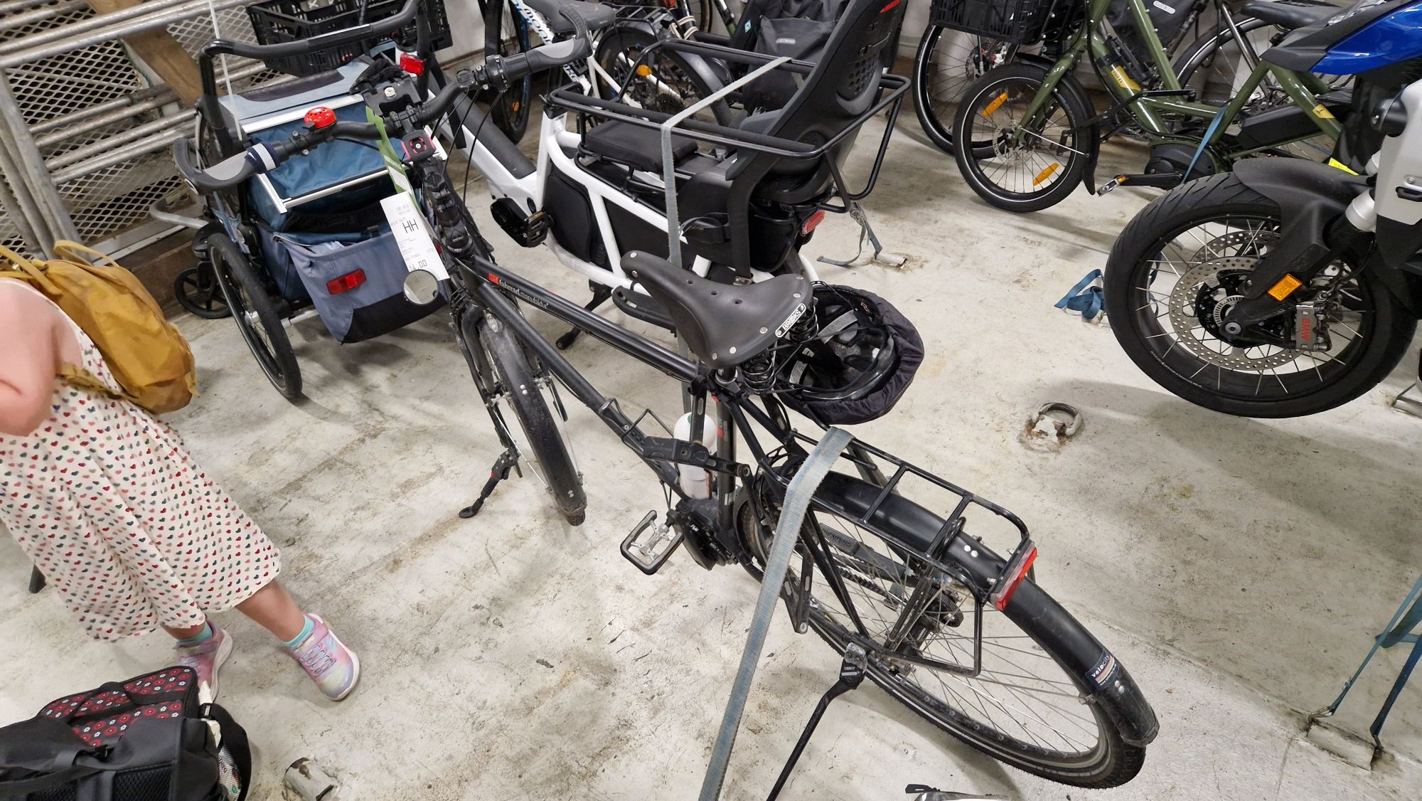
Securing my bikeLeaving BergenBye Bridge in BergenView on the hillsMy sleeping place on the shipHuge transmission towers near HaugesundApproaching Stavanger harborMy dinnerGoodbye Sun, Goodbye Norway 🇳🇴
I was filled with joy and happiness, and I’m looking forward to arriving at home tomorrow. This concludes my 2025 bike journey, and I’ll post about the travel back home to Braunschweig.
Tuesday, July 15th. I was greeted by sunshine in the morning and basically perfect weather. My morning routine was a bit slower than usual and it took me 3 hours to get ready for the cycling. I “sacrifice” a lot of time in the morning, so everything is properly packed for the evening.
Shelter on the next morningLeaving the shelter
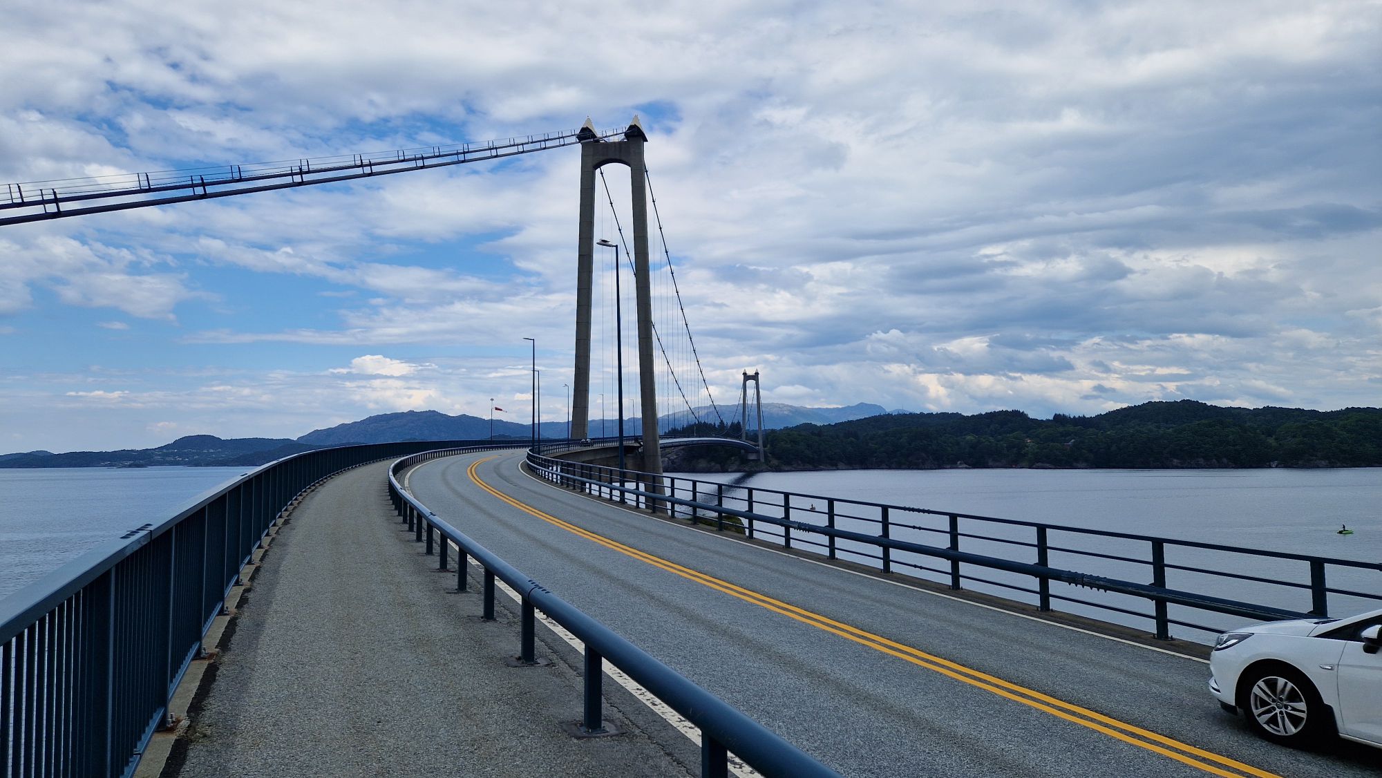
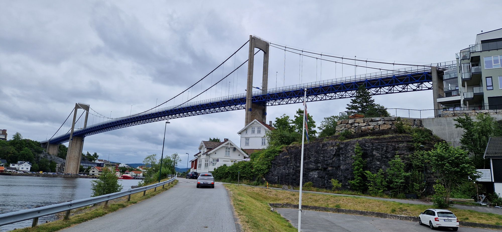
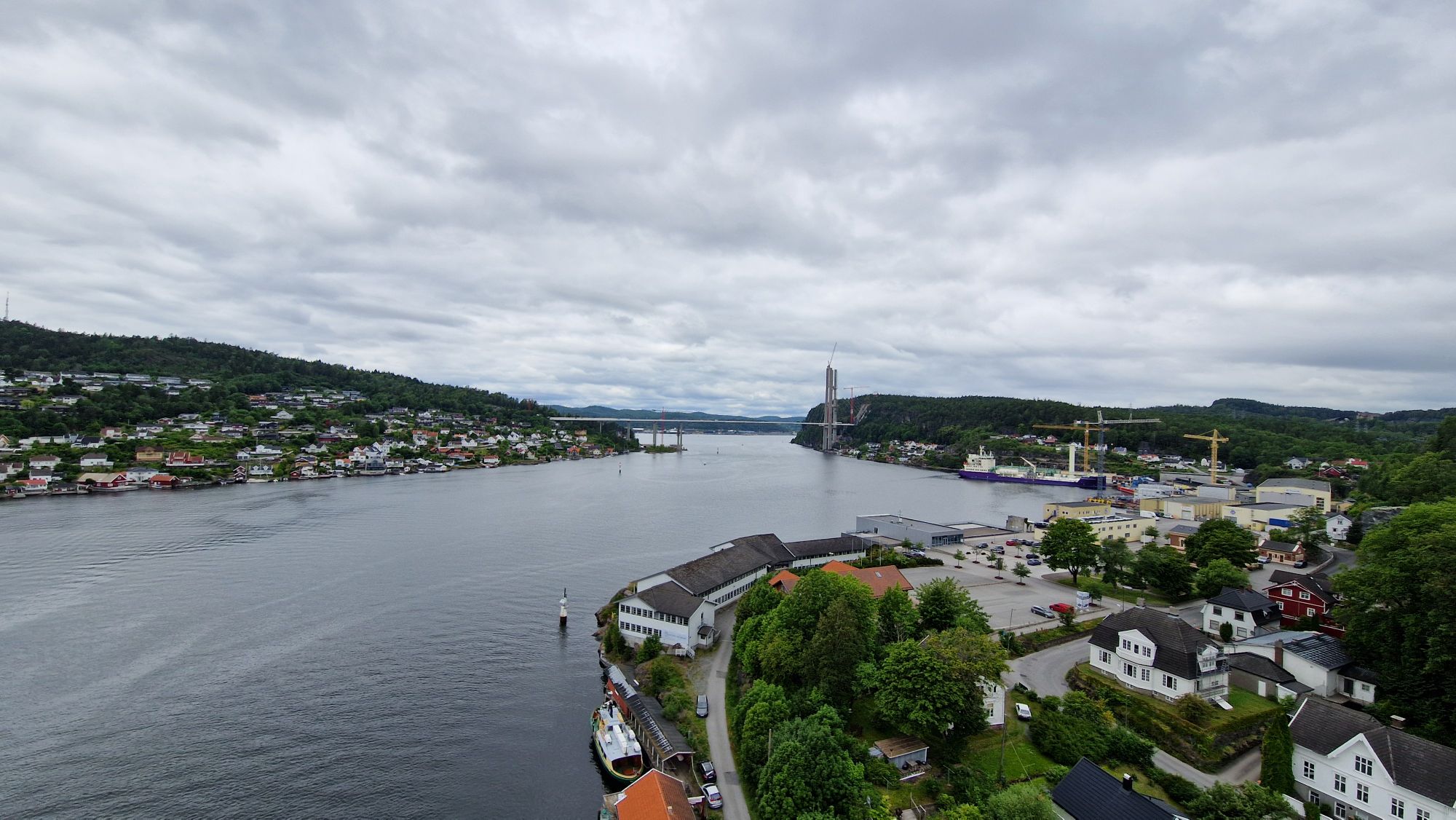
I left the shelter around 10am and was looking for a toilet because there was none. I was hoping to find one at the local church but had no luck. I met there a local elderly man and had a very interesting chat with him for about 20 minutes. He told me about his town and the region I’m visiting – truly a very educated man. We said goodbye to each other and I continued my route towards Leirvik. Few kilometers before Leirvik, I crossed three truly amazing bridges: Spissøybrua (280 m), Bømlabrua (998 m) and Stordabrua (1077 m). I took hundreds of photos before it started raining, just after I passed the bridges.
Church in BømloRoadkill frog, RIP ✌️✌️BømlabruaView southView northStordabruaView westView east, rain clouds in the distance
I met Doug, a cyclists from Australia/UK and we had a chat about our routes. My visit to Leirvik was short and I moved on despite some moderate rain. My way to Fitjar was a bit exhausting: I was tired and the rain came and went faster than I could change clothes 😅 About 10 km from Fitjar there was some heavy rain which really convinced me to stop and seek a camping spot. At 7pm, I’ve found one camp site 3 km from Fitjar, however, the owner wasn’t available. Just around this time, the rain stopped, sun came out again and I reconsidered my decision to call it a quit. I tried to reach Sandvikvåg to get to the last ferry in order to save some time for the final Bergen approach.
Tower in LeirvikView after rain was gone, near FitjarView on entering FitjarFerry arriving at SandvikvågDeparting SandvikvågView on the fjordApproaching the destination harborBack on Route 1
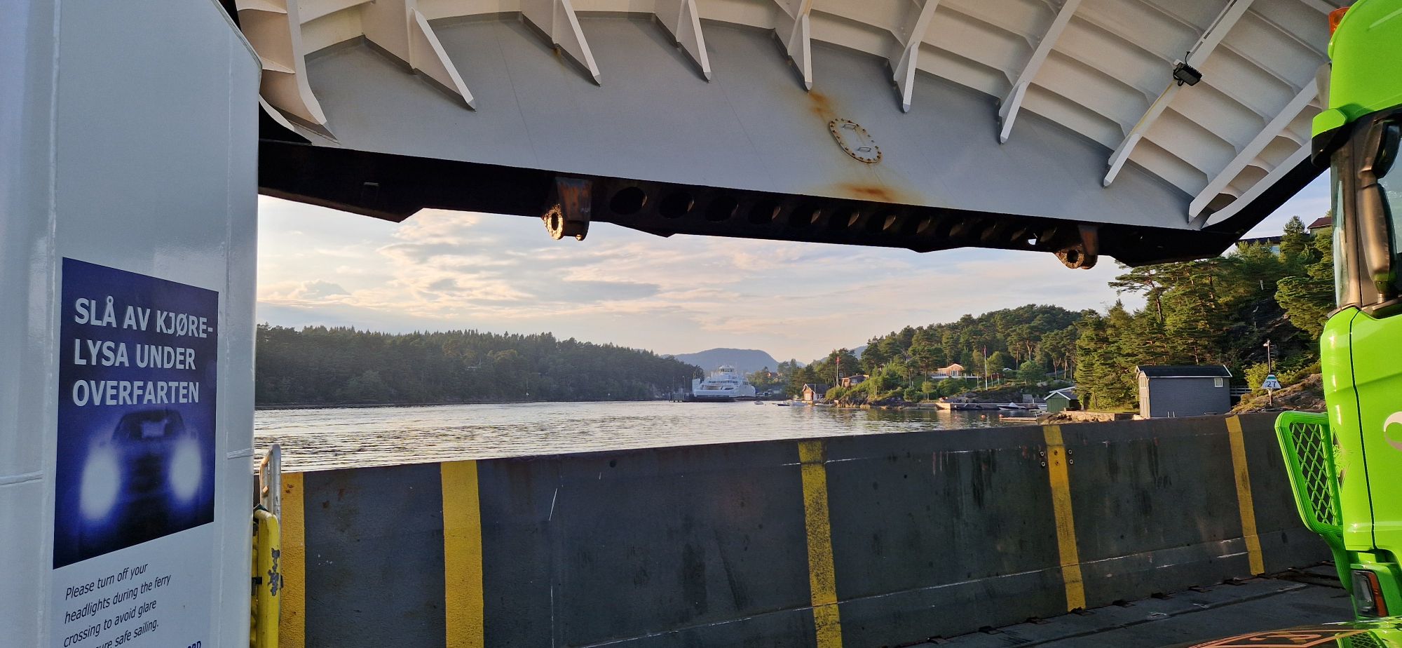
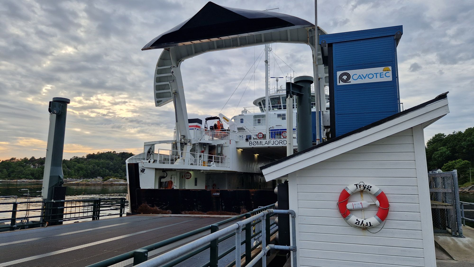
Luckily, in the meanwhile, the weather got much better and I was able to catch the ferry from Sandvikvåg to Haljem at around 8:30pm. The ferry was – again – free of charge and got me over the fjord in just 40 minutes!
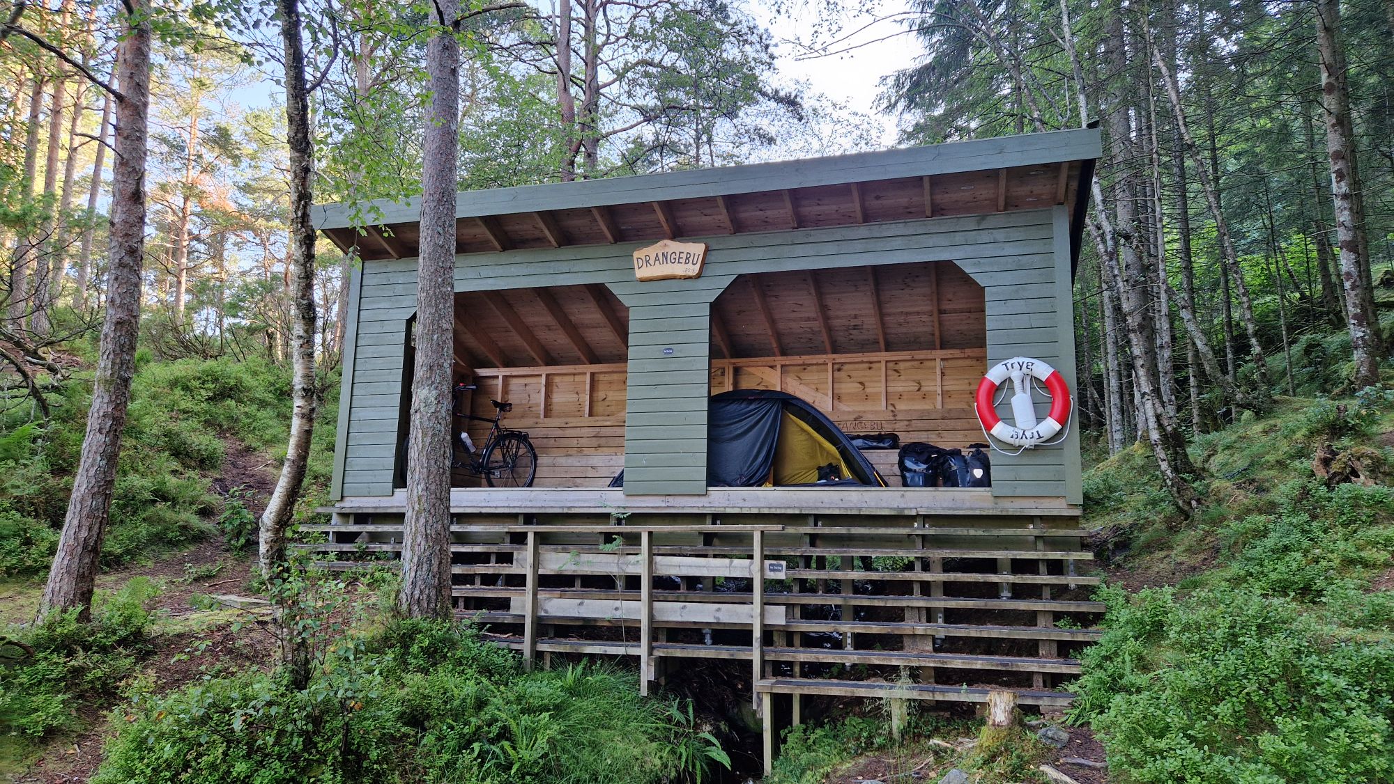
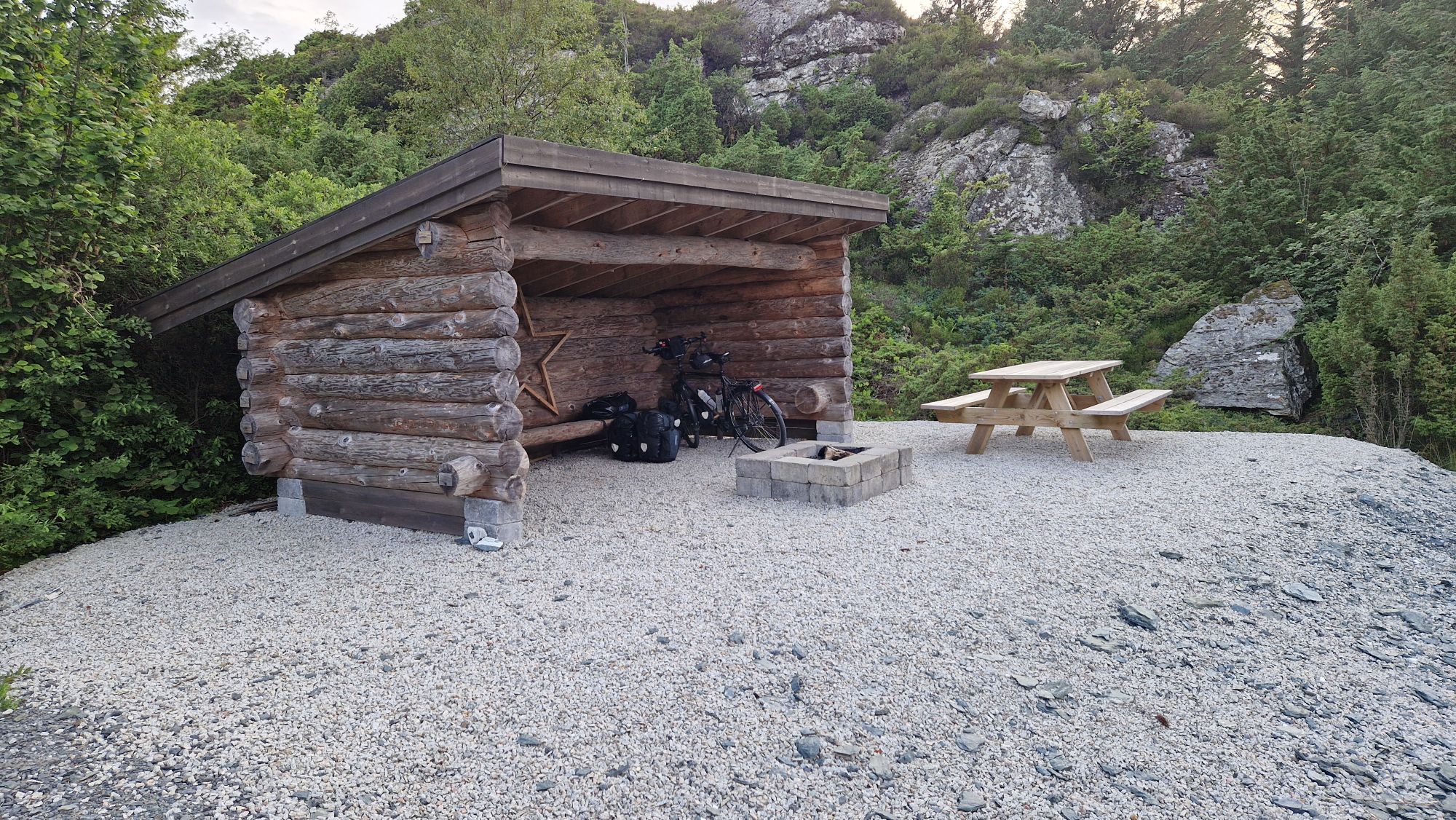
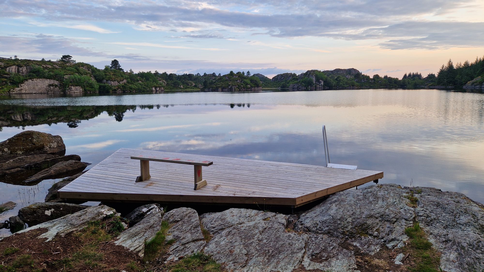
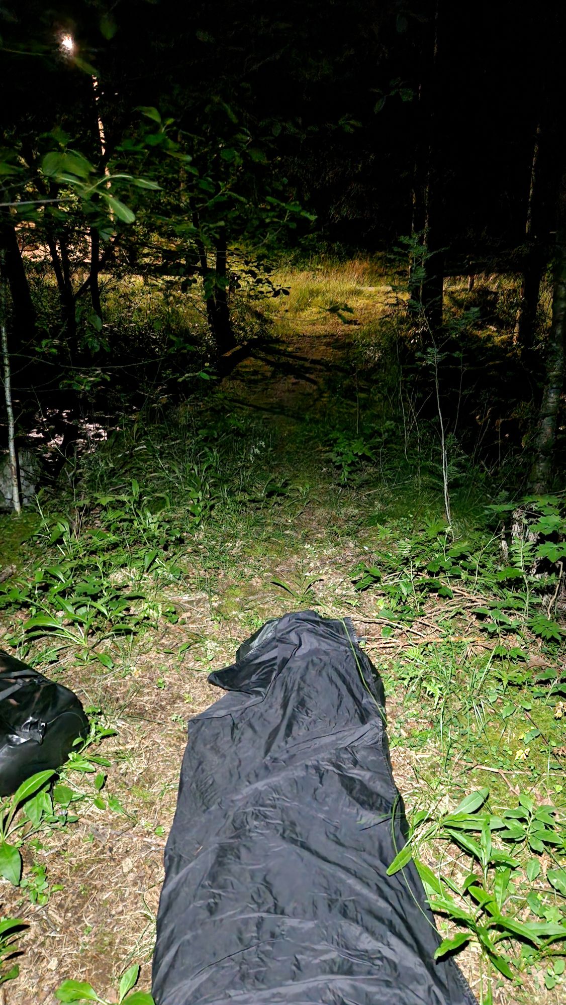
At this point, I’ve been way ahead of my schedule and I had to plan the next steps “on the fly”. There was a shelter some 10 km away from the port, so I tried to get there before it really got late. I’ve visited Osøyro on my way and had to battle some difficult and steep hills before getting to the shelter place near Søvik around midnight.
Views on the roads and hills im the eveningSculpture in OsøyroIt said “Northern Explosives Dog”Views on a lake near Søvik, around midnightSetting up the tent before I get mangled by mosquitoes
Setting up the shelter wasn’t easy: it was located on the edge of a nearby forest and lake. I took few wrong routes and had to search for the shelter in the darkness. After finding it, the shelter was difficult to access but barely large enough to hold my tent. There were many insects around, including one peck, so I had no time for my evening routine and just retreated into my tent.
I’ve checked the return route from Bergen back to Germany but everything looked grim: the Bergen/Oslo train was full (no bikes allowed) and it took too much time (7h) for the route, resulting in a bad connection of trains. My second choice was a ferry from Bergen to Hirtshals, but it seemed impossible and out of reach due to time constraints and a very tight schedule. Anyways, I went indecisive to sleep…
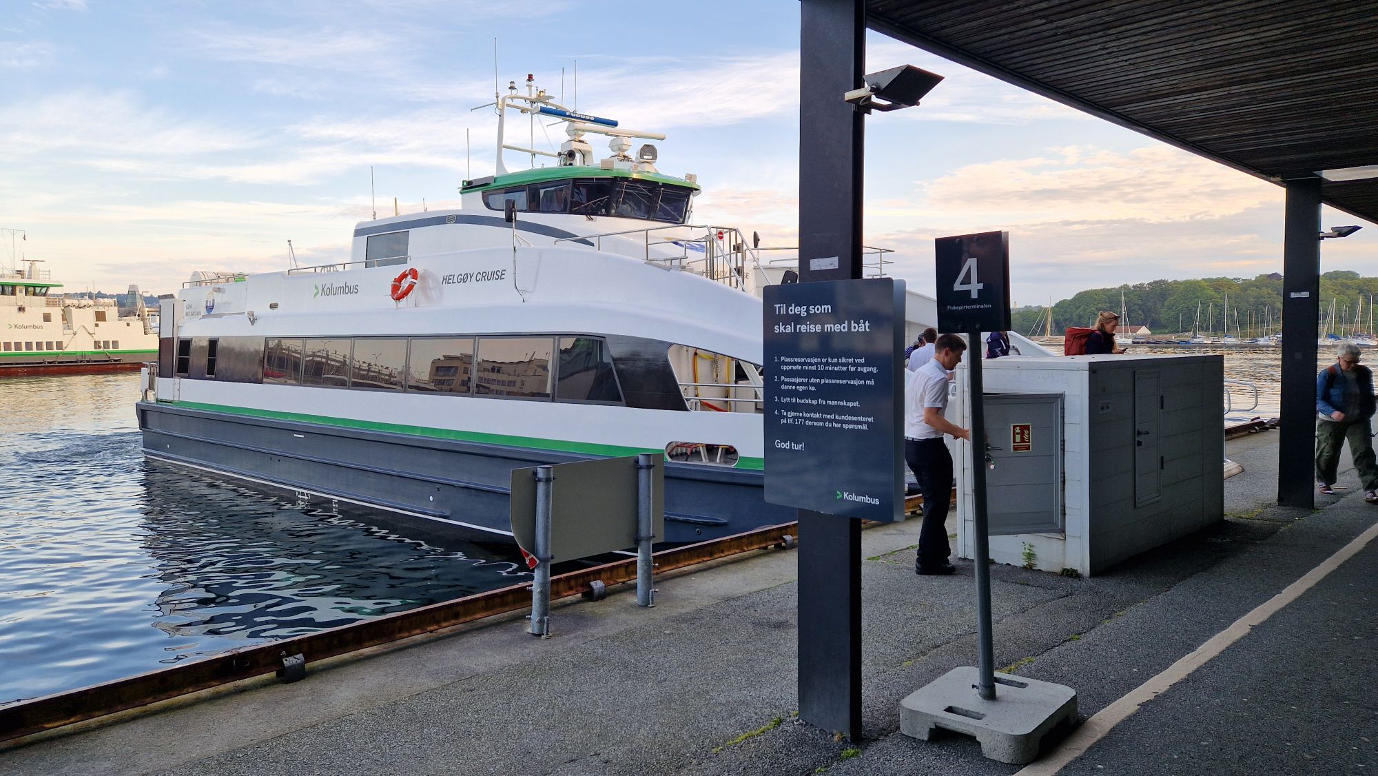
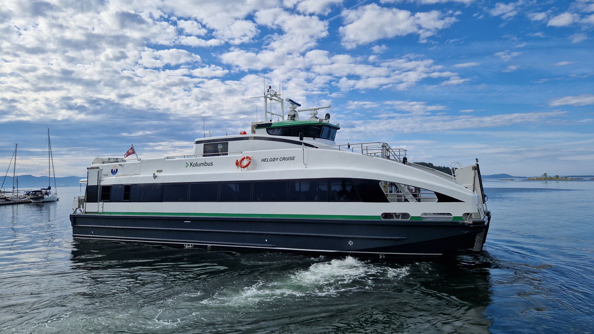
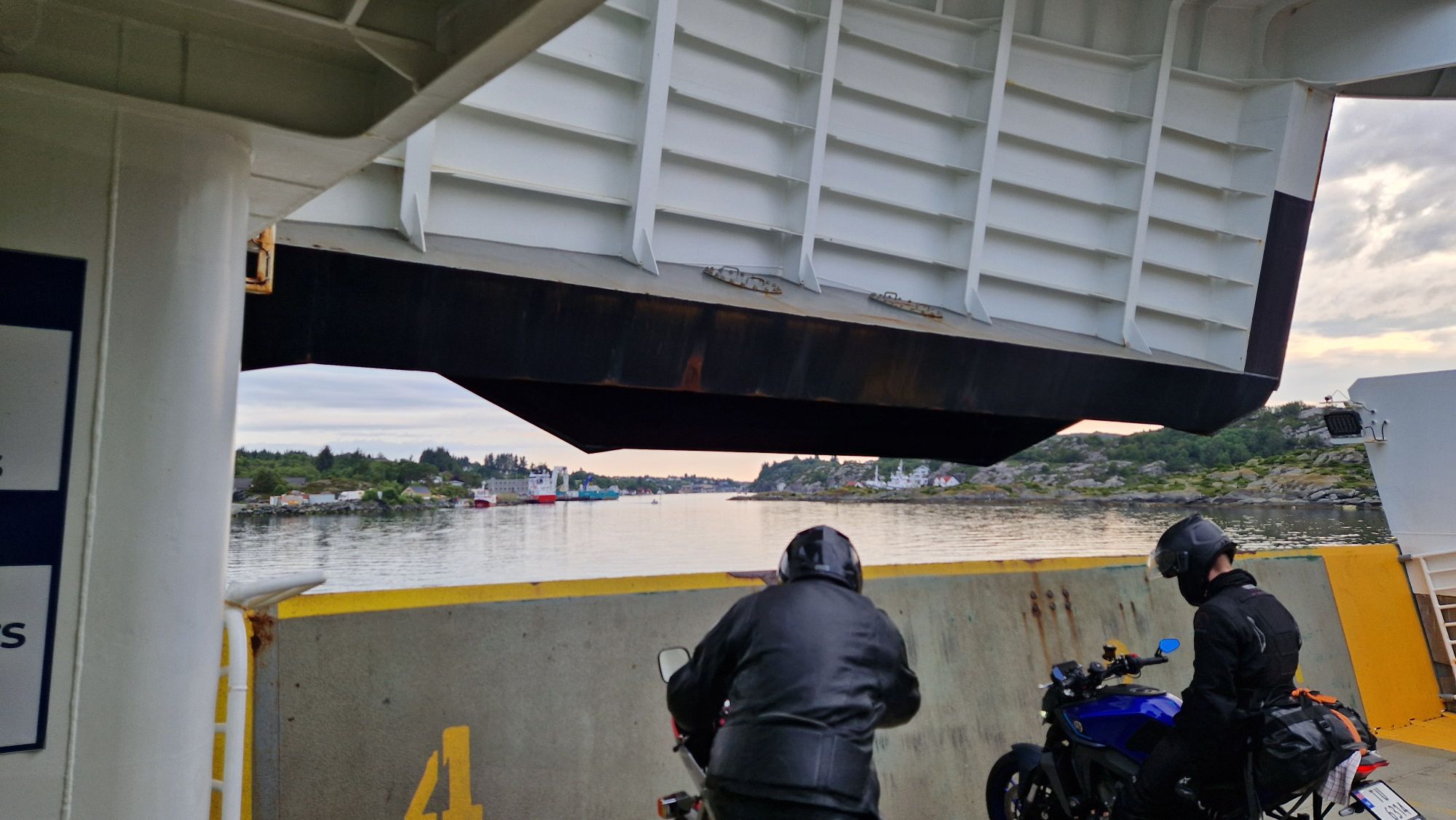
Monday, July 14th. I woke up very early in the morning around 4:50am just to be ready to leave around 6am towards the Stavanger harbor so I will be on time to leave to Nedstrand at 7:15am. I got there on time but had only very little time to photograph interesting stuff on route. The fast ferry arrived on time and brought me to Nedstrand, where my tour continued. The costs for the ferry were 177 NOK (around 15 EUR) when ordered on-line via internet. The harbor terminal Stavanger Fiskepirterminalen was easily to get to, and the crew helped me to get the bike on board. The transfer time was 1h45m.
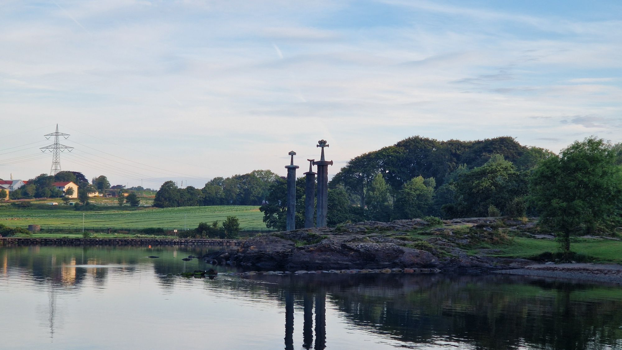
Three swords at a fjordAndemor sculpture and an owl sculpture in the backgroundSpeedboat arrivingComfortable seatsShip departing from NedstrandArrival in Nedstrand
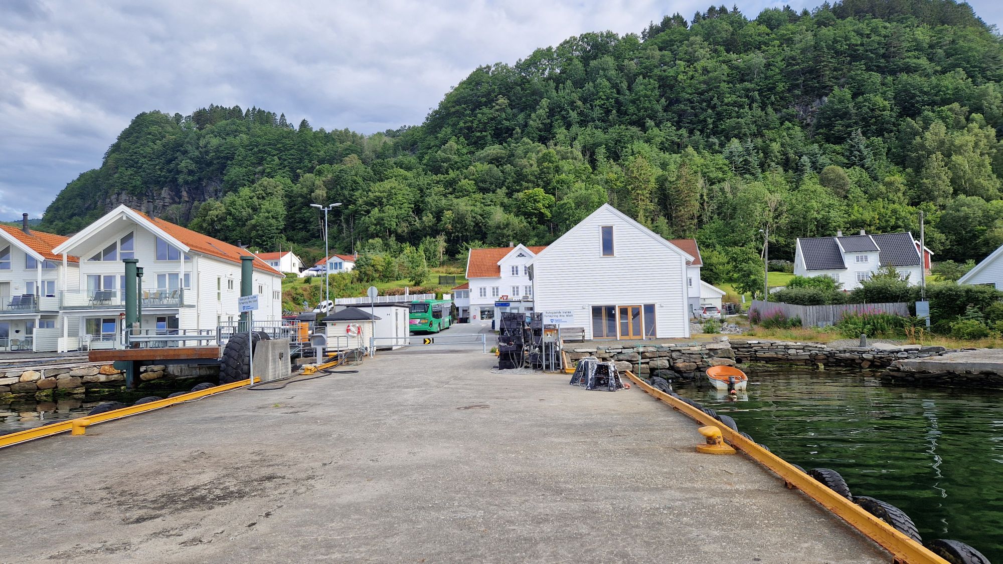
The route from Nedstrand to Haugesund was actually fine for cycling: no steep hills, just regular county roads with the usual hills. There was not much traffic going on that day and the weather was very favorable. I reached Haugesund in the afternoon around 5pm and after checking out the famous spots, I kept cycling towards Buavåg, where another ferry would transfer me over the fjord. I started panicking how to get a ticket, but luckily, the ferry was free of charge and transported me to Bømlo in about 40 minutes.
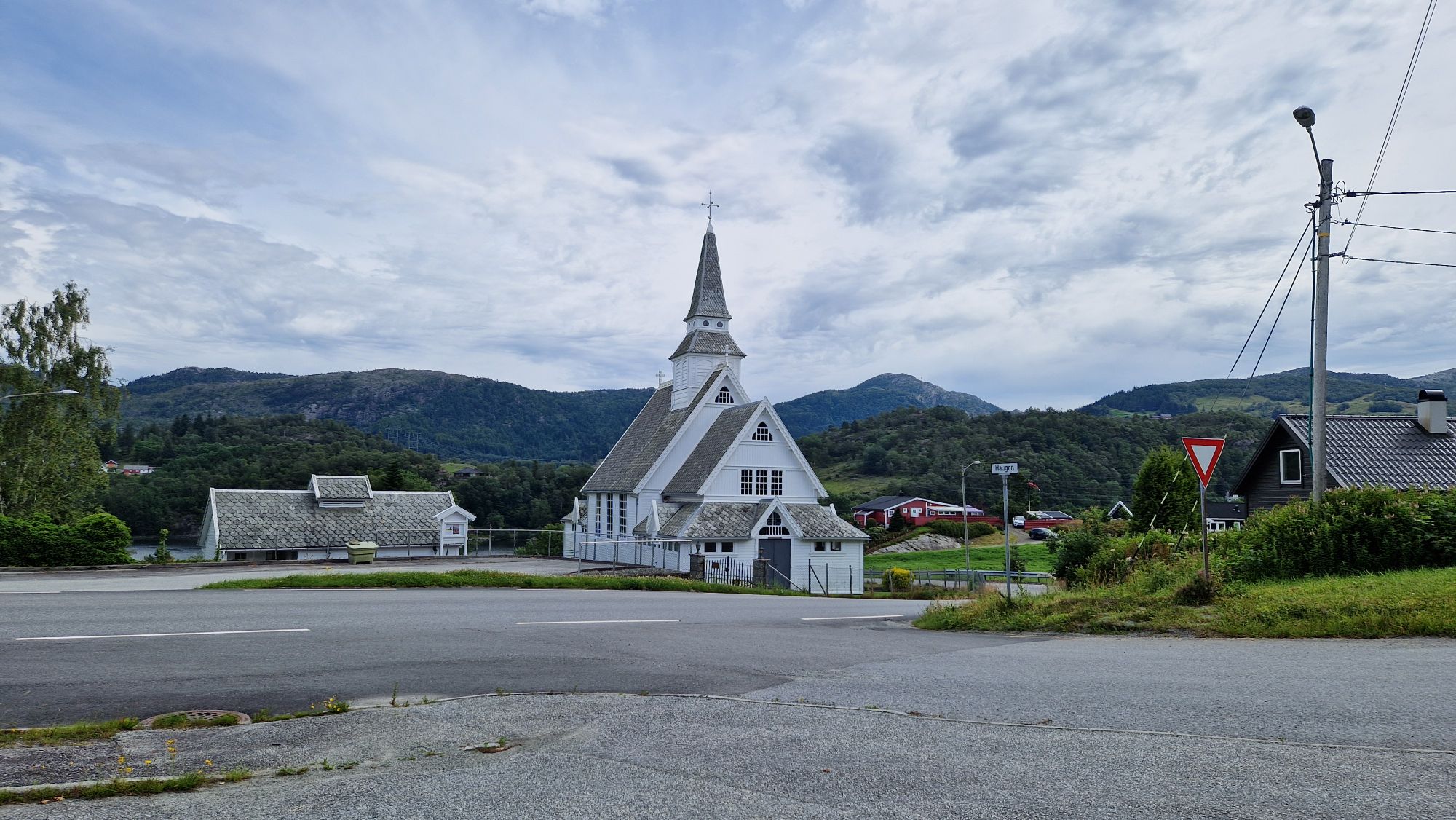
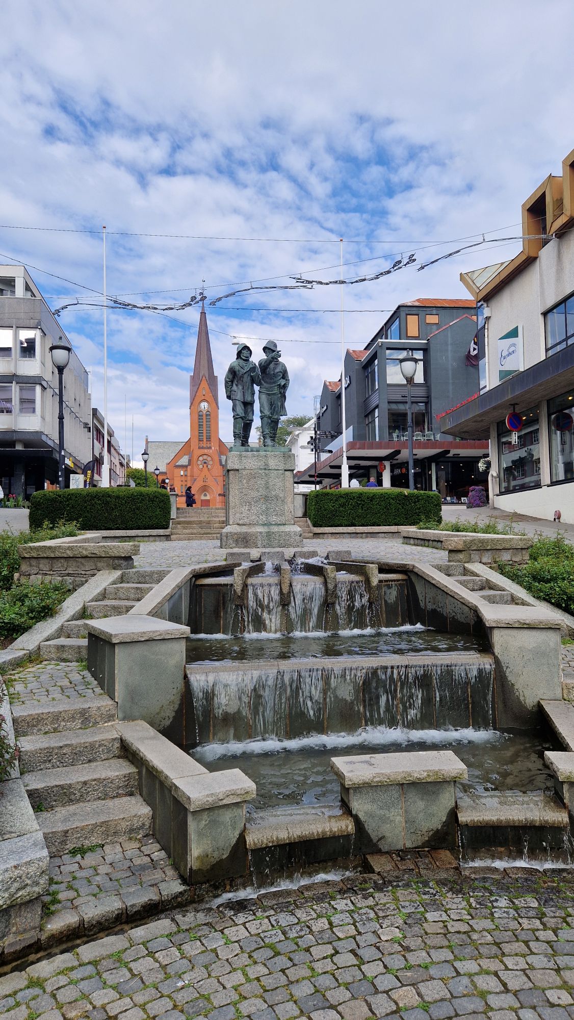
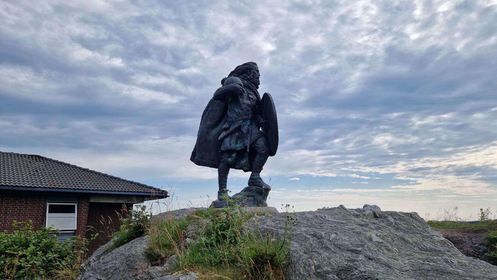
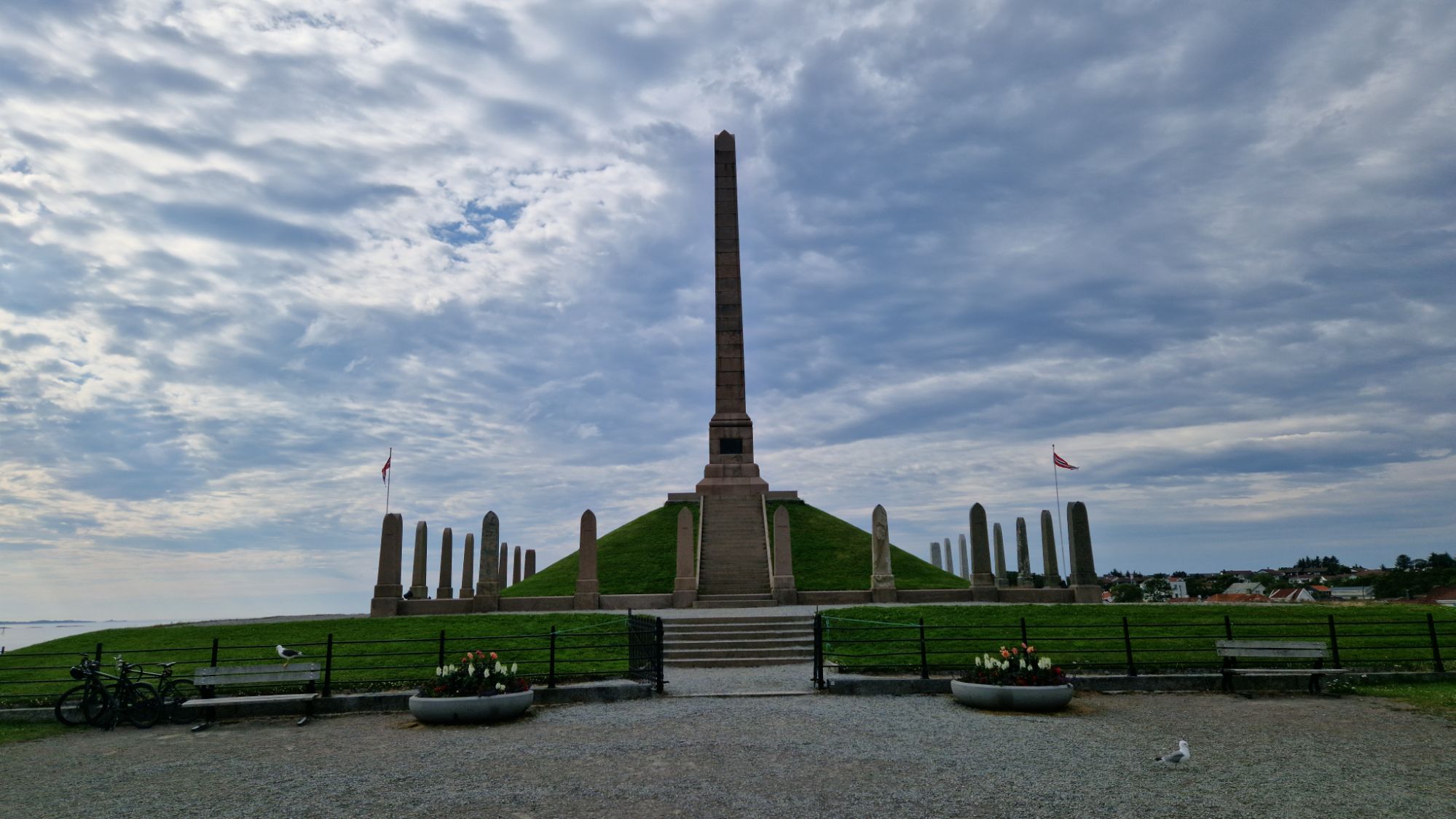
Road and landscape near NedstrandChurch near AksdalFishermen fountain in HaugesundEpic statue, King Harald FairhairEpic national monument in HaugesundAnother historical memorial place near HaugesundFerry arriving at BuavågCrossing the fjordArriving at BømloView on Langevåg/Bomlø
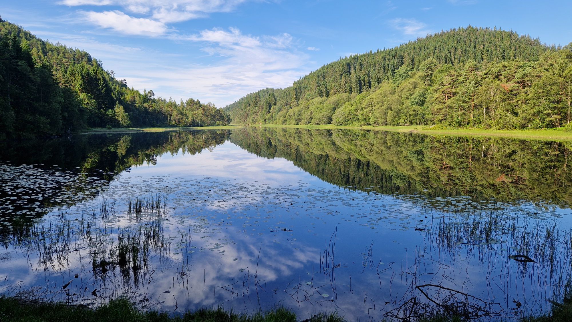
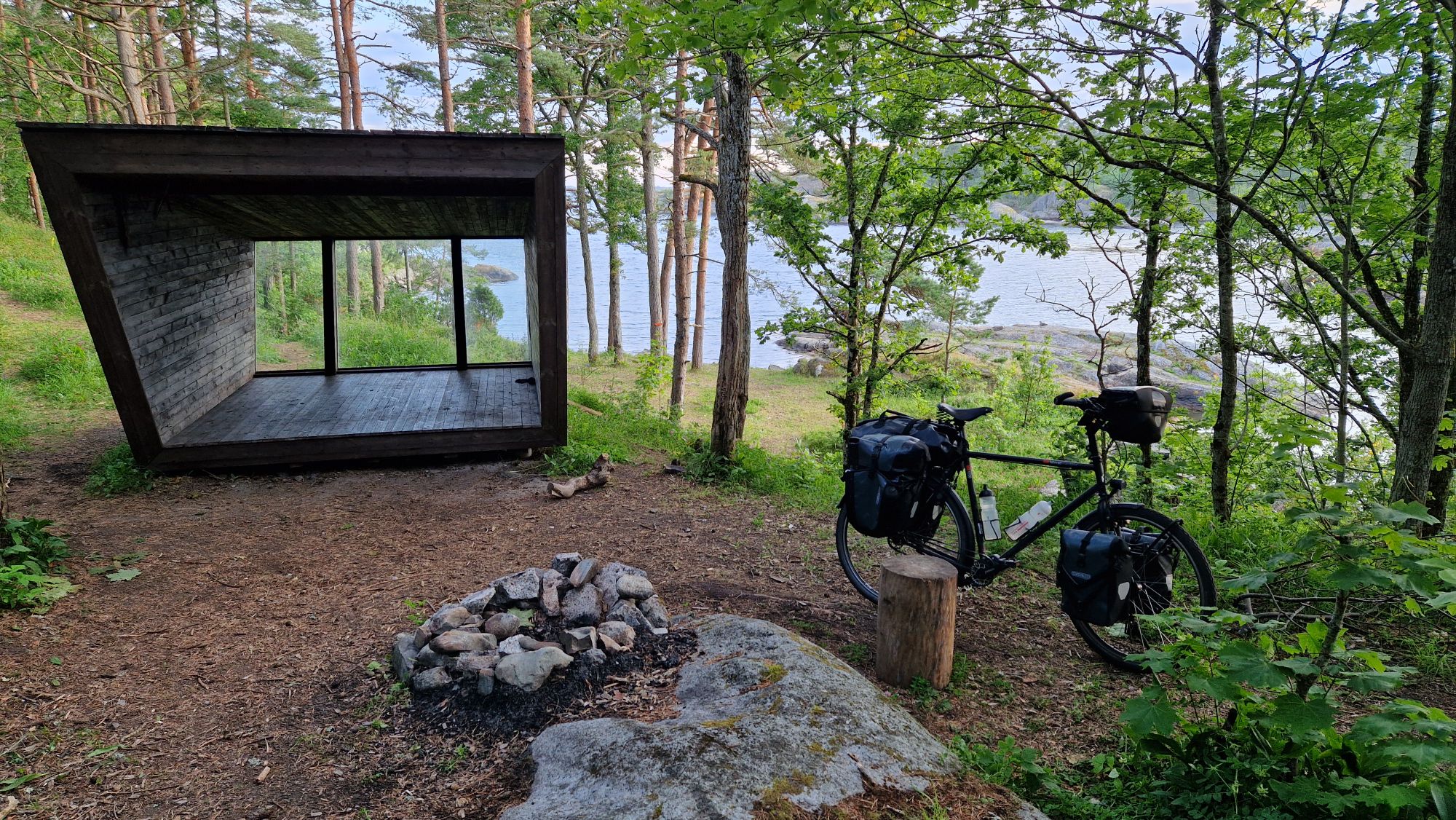
I found myself ahead of my schedule and found a shelter just 10 km away from the harbor. The shelter was close to a nearby lake where I could get a bath. I was alone there and enjoyed the time before being forced to retreat into my tent by endless flying insects and mosquitoes.
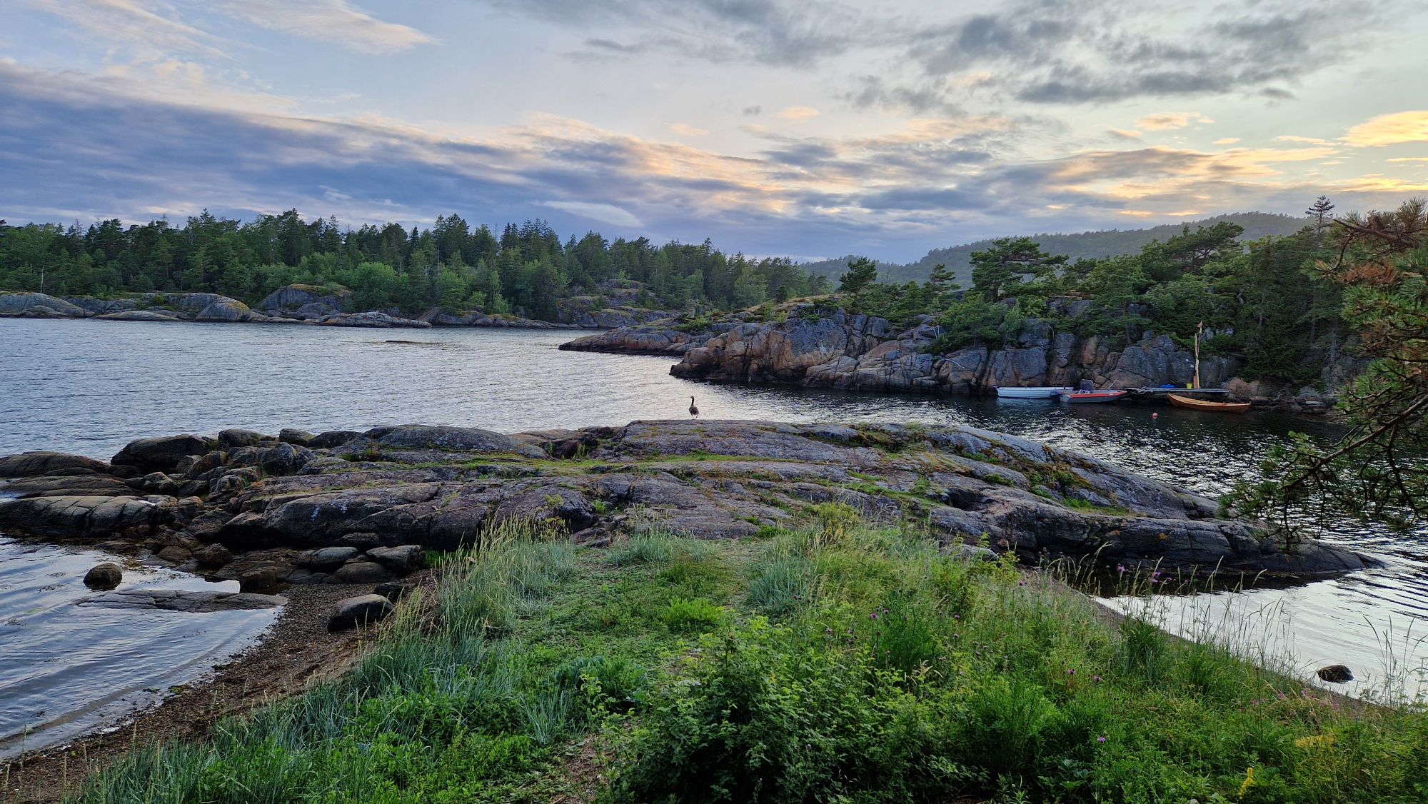
The shelter near BomløNearby lake… nice!
95.65 km, 8h00m, 11.95 km/h average, 49.14 km/h max
Sunday, July 13th. The weather changed overnight and brought some rain. I left the camping site around 9am and cycled randomly towards Stavanger. I stayed mostly on roads and partially cycled on Route 1. I skipped the gravel road parts due to rain and mud.
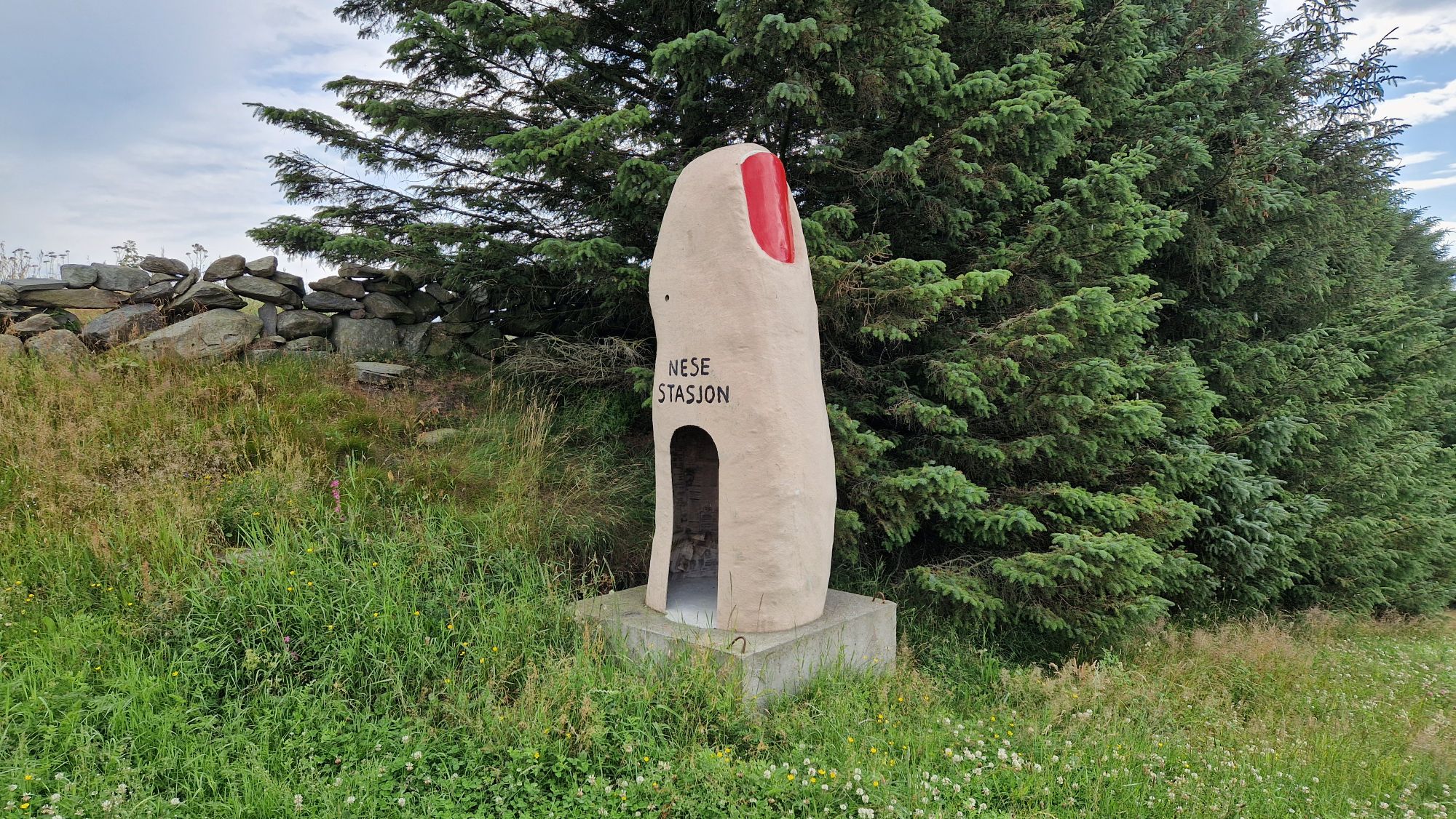
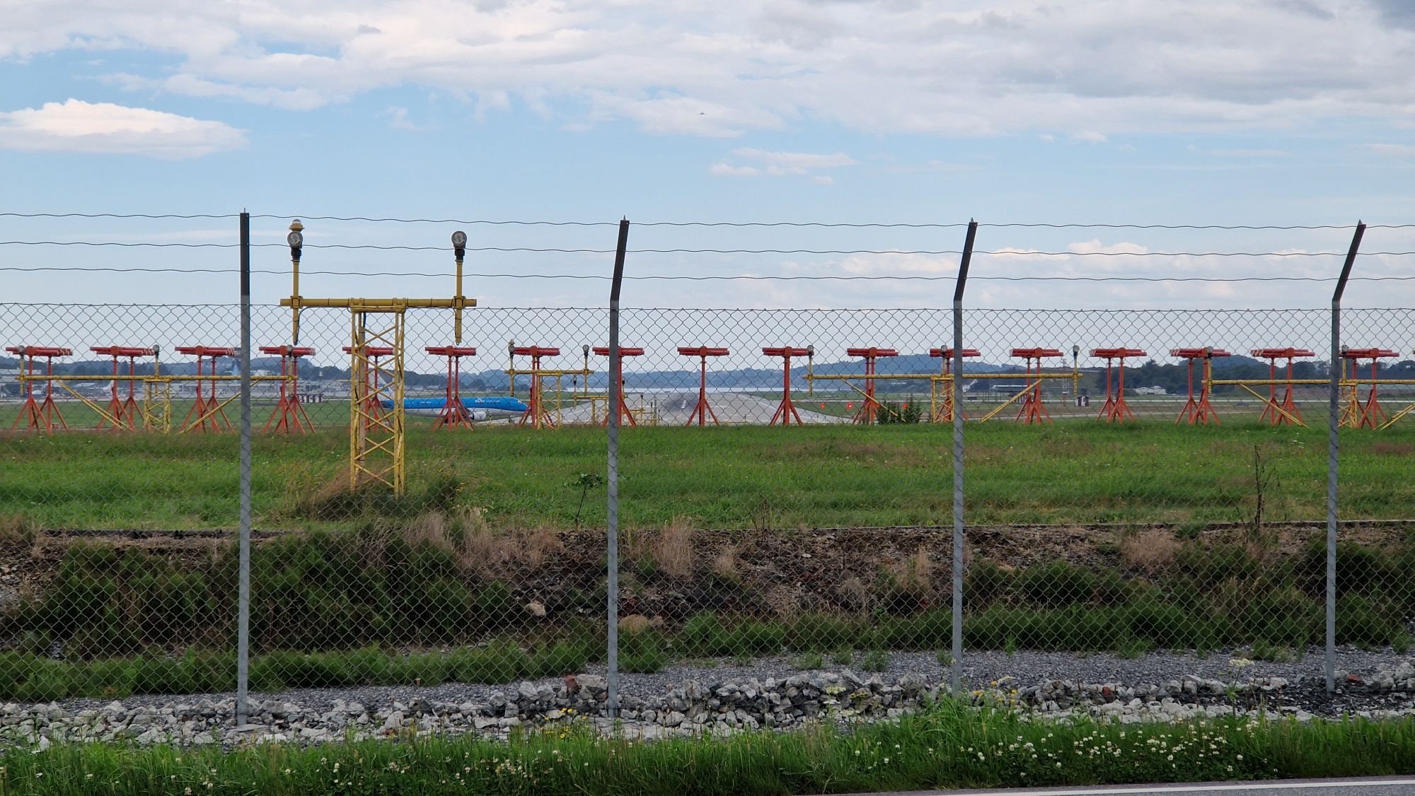
Bye bye, hillsSome radio stationCrossing of a small bridgeA fingerAirport Stavanger
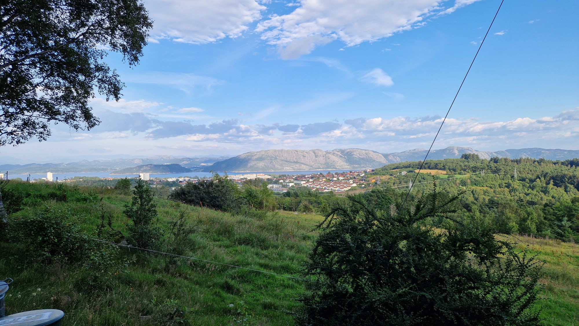
The terrain was mostly flat, and it was a welcome relief for my legs. I arrived at a place near Stavanger where I visited friends and stayed there overnight. They made some super delicious Moroccan food with best spices and ingredients. I was just overwhelmed by their hospitality and kindness. Awesome! The weather was really amazing in the afternoon, I was amazed by the views from a nearby hill.
We talked about food, travel, life, test equipment and our future plans before going to sleep. Unfortunately, I needed to leave very early in the morning to catch a ferry to Nedstrand hurtigbåtkai.
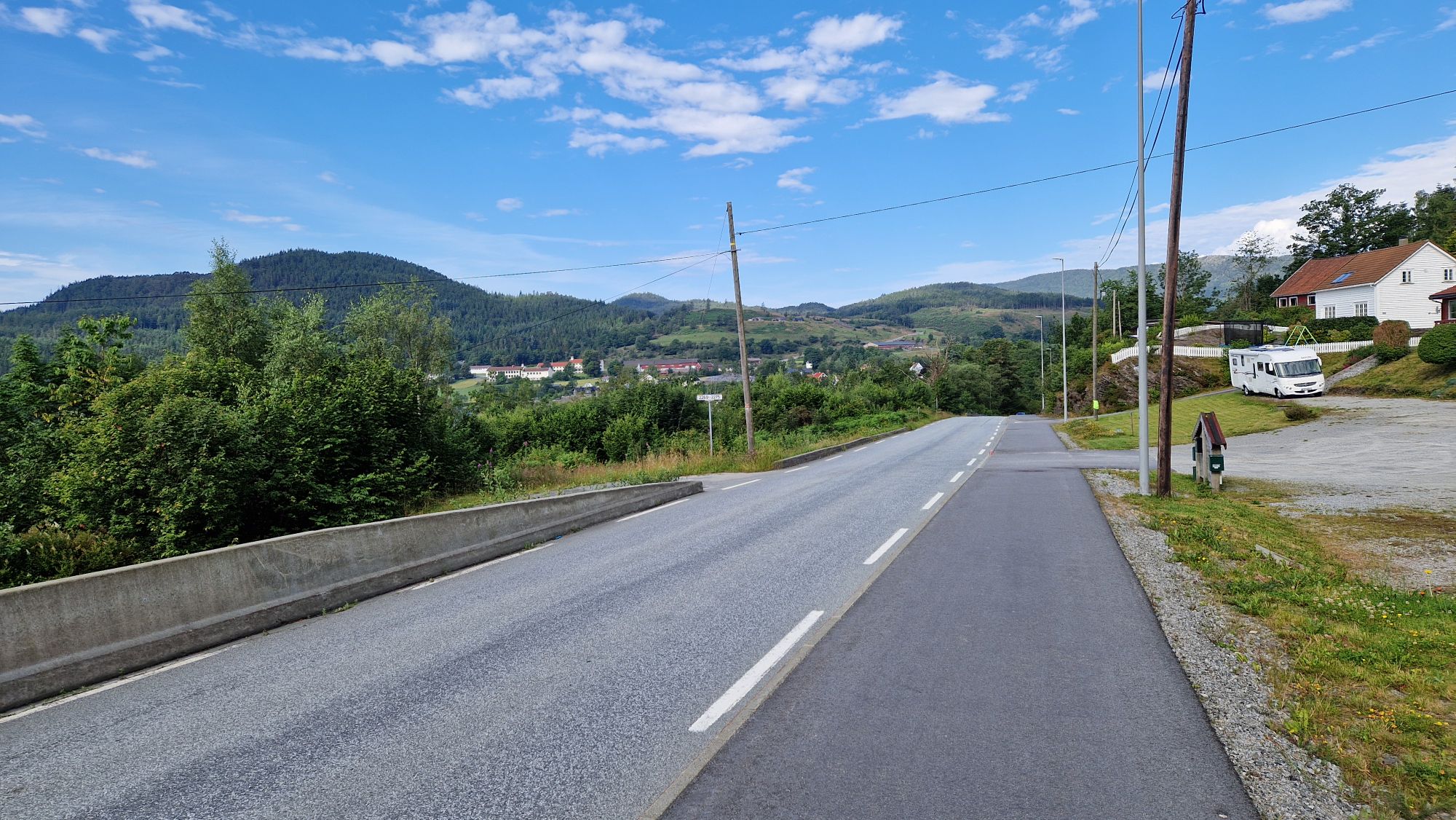
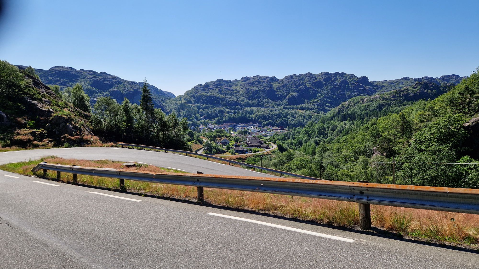
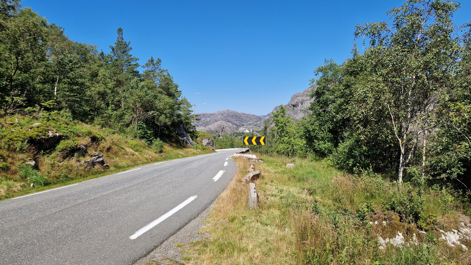
Saturday, July 12th. This was the most difficult and most epic day of all of my current journeys. Woke up early, and I had perfect sunny weather peaking at 25-28 °C. I left Flekkefjord around 10am and headed towards Egersund, which was 72 km away.
Road near Flekkefjord
Shortly after Flekkefjord came my first ascent. It took me about an hour of pushing my bike. Unfortunately, I have no information about the names of the hills or heights, so please bear with me. The streets were in very good condition, and the car drivers were super careful with overtaking and very friendly. The downhill route was very fast and led to a village Åna-Sira, which was located in a valley.
A milestoneBridge near Åna-SiraView from the bridgeNorth Sea cycle route sign in Åna-SiraFrom Flekkefjord to Åna-Sira
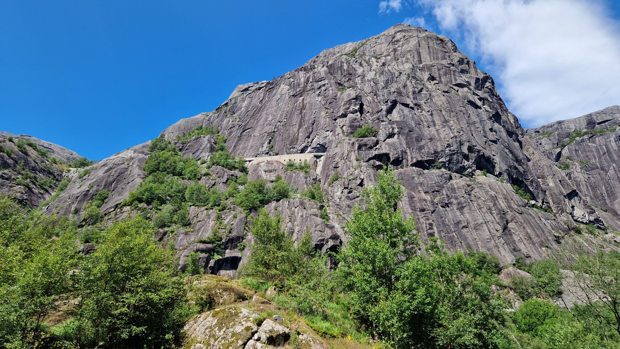
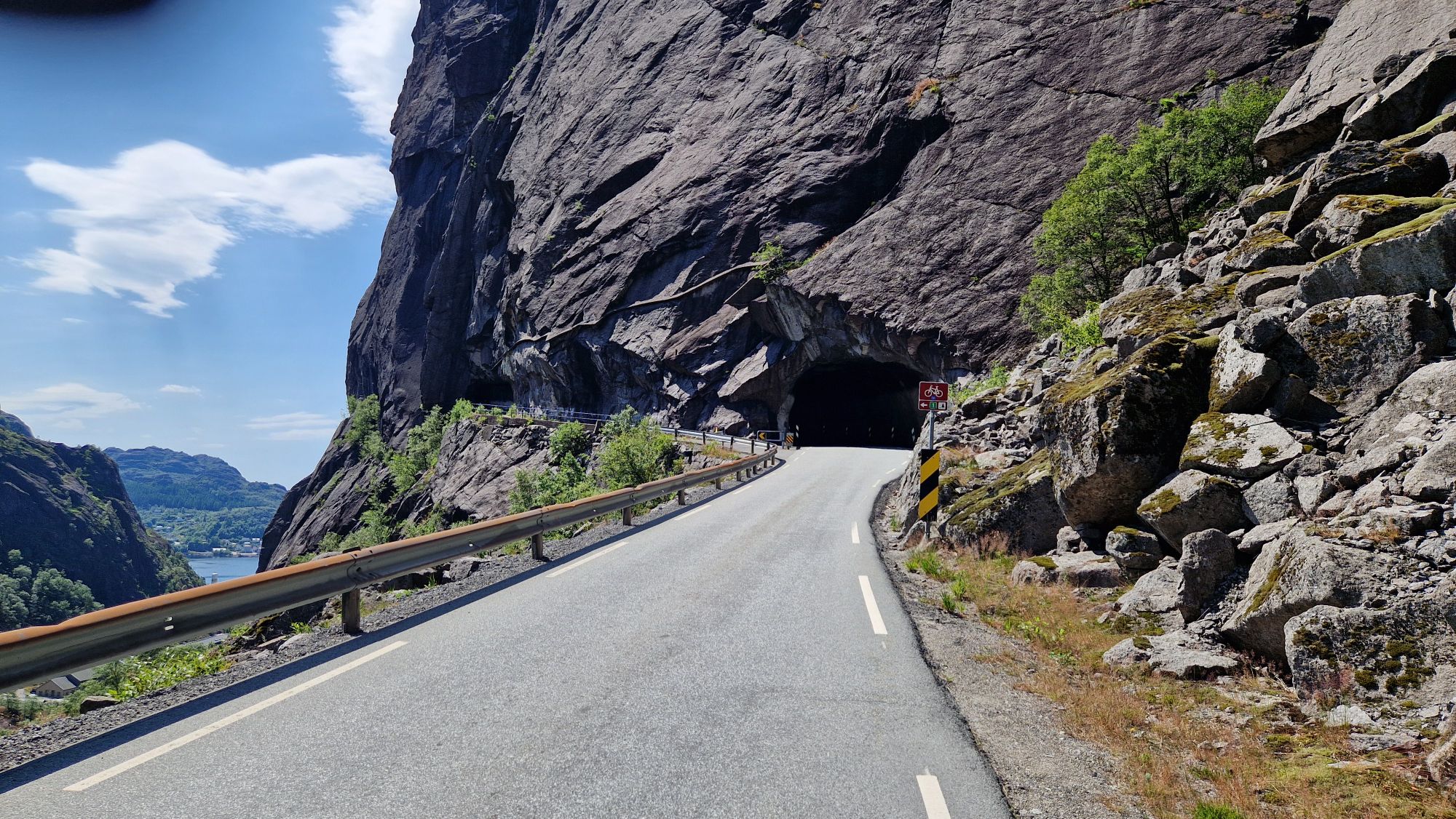
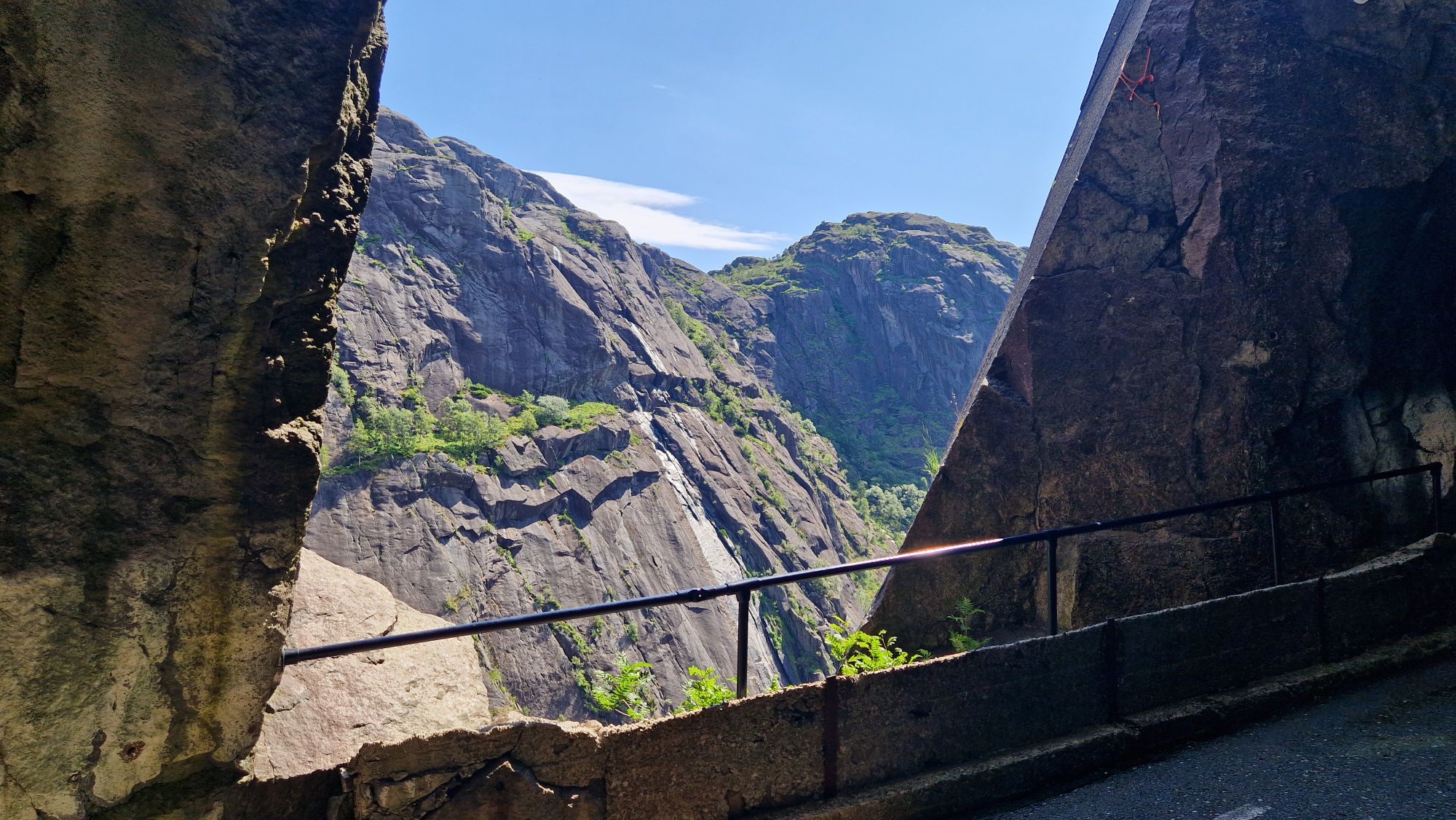
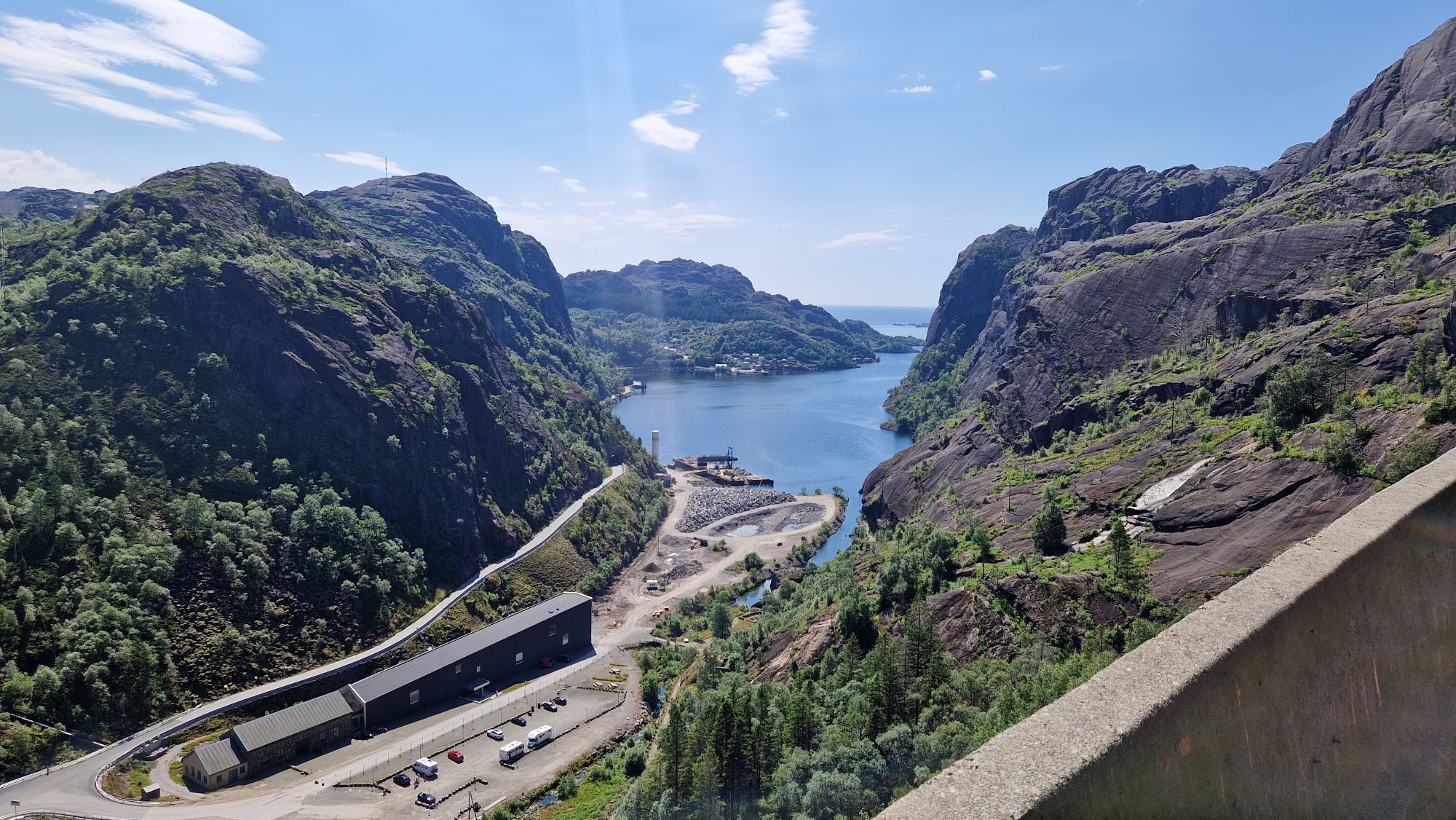
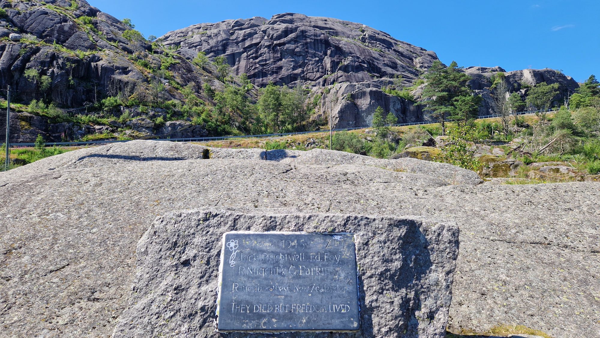
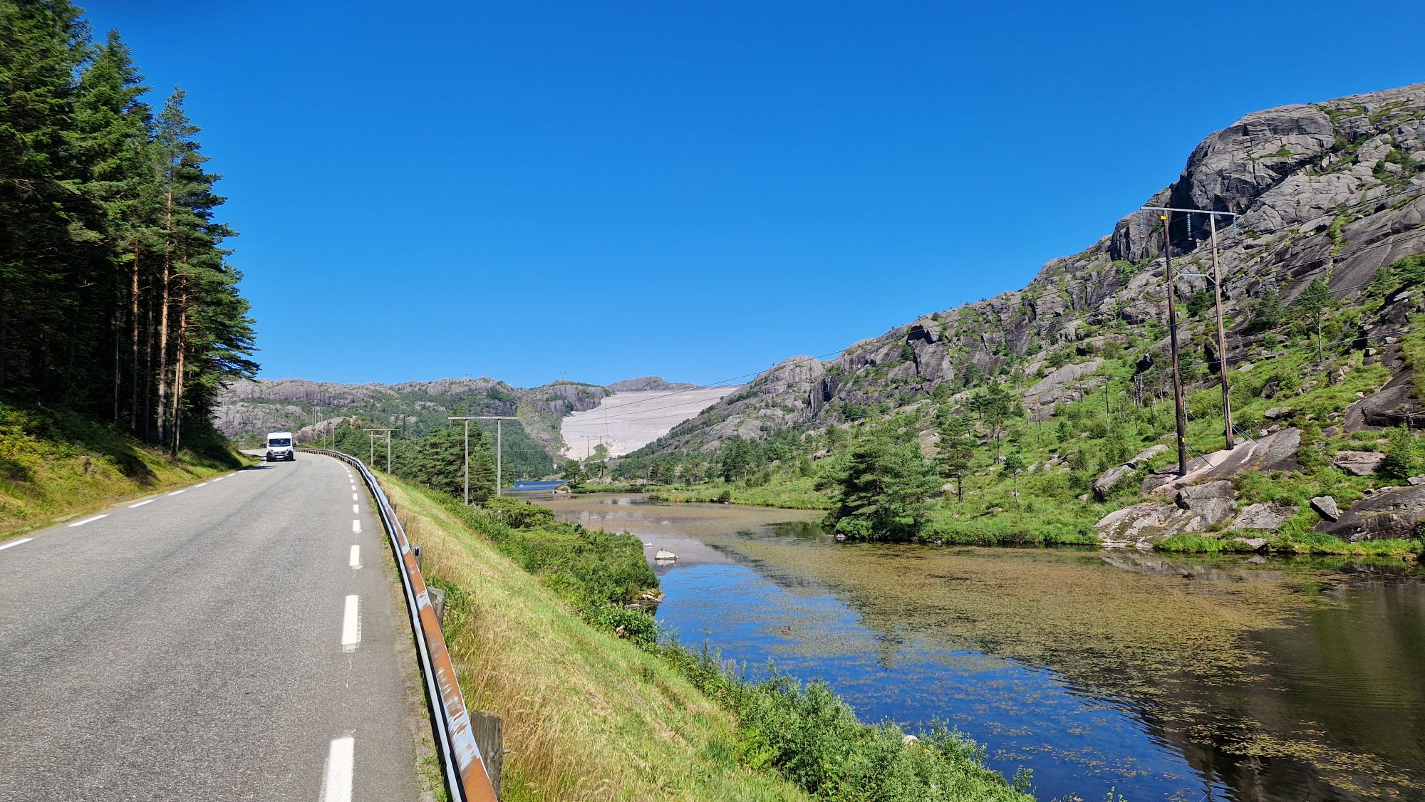
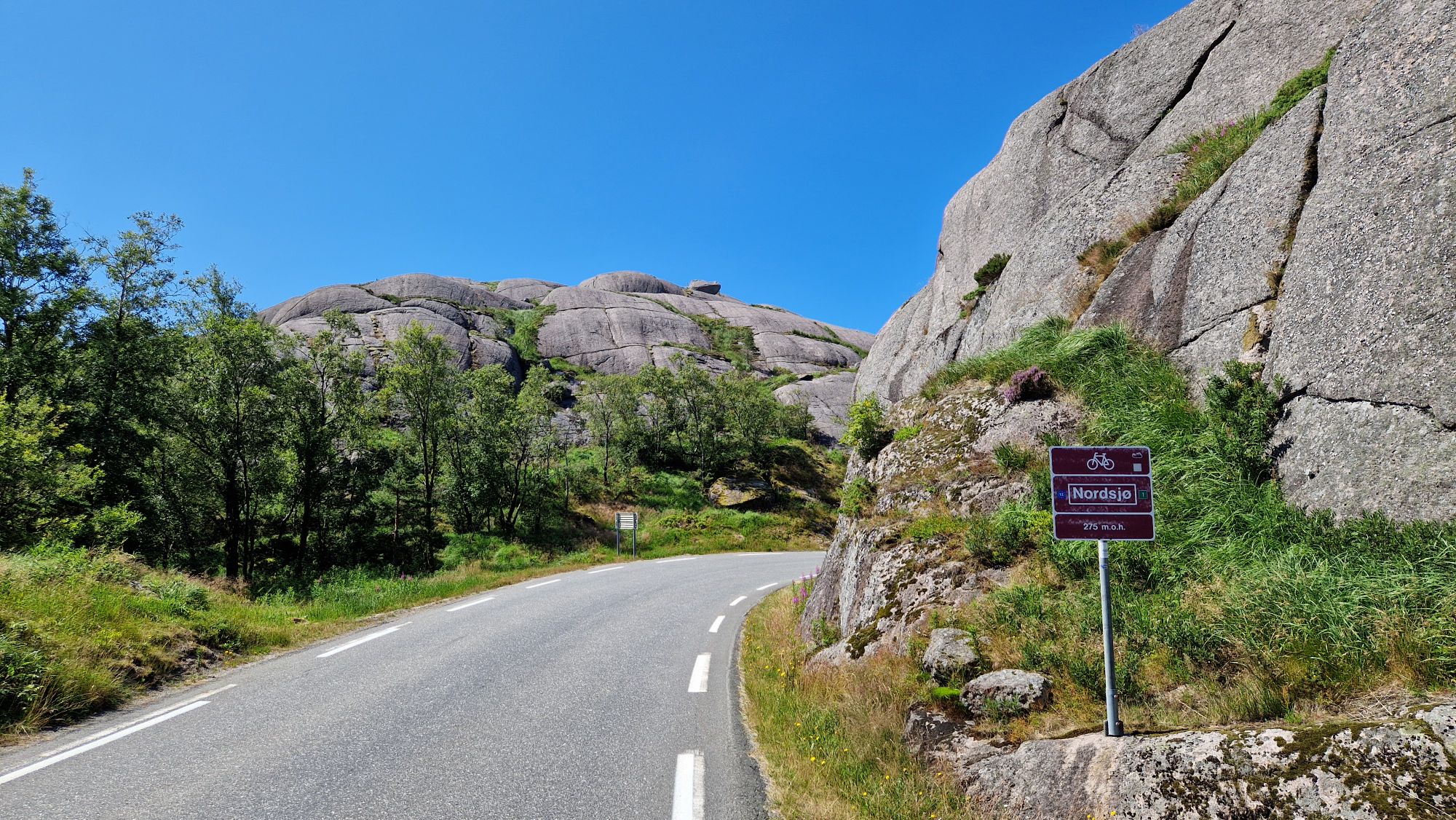
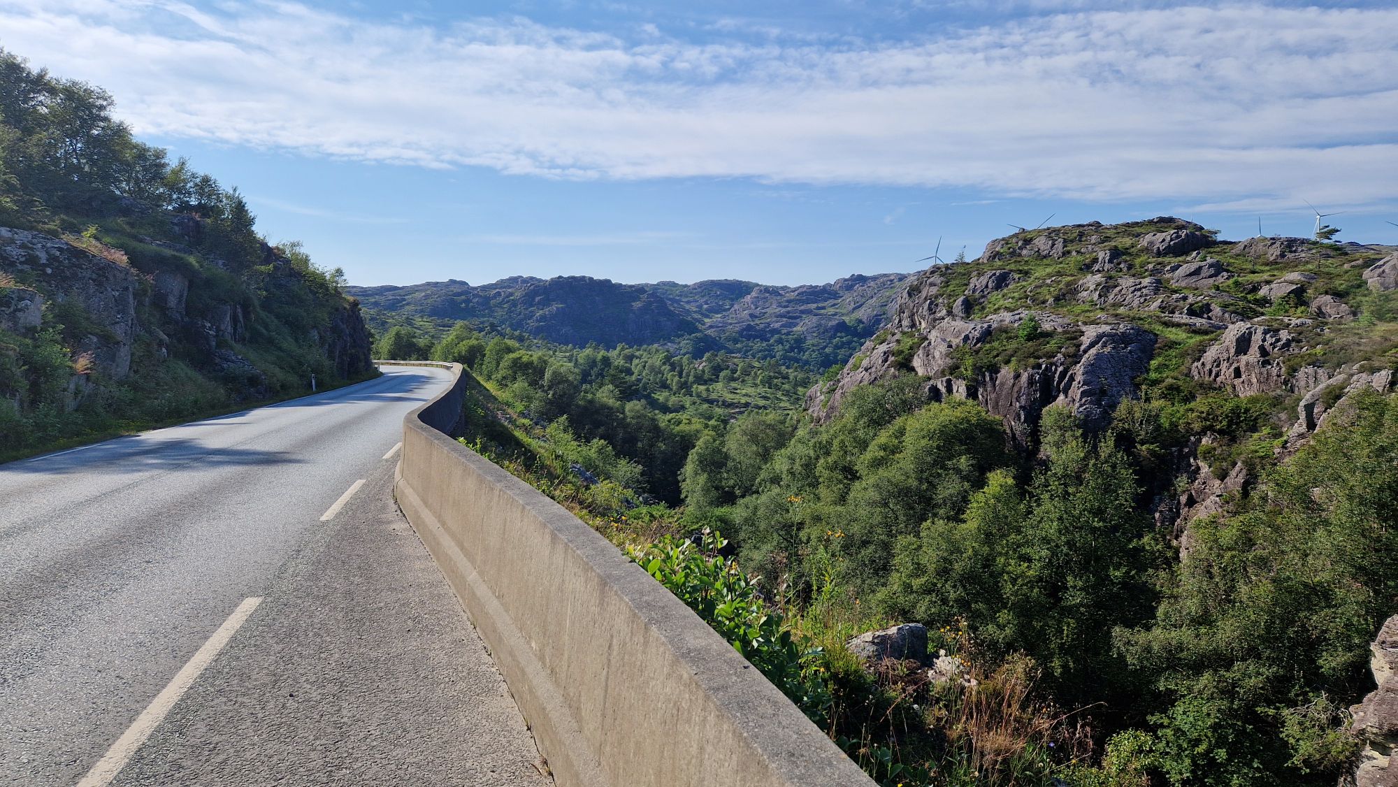
I passed Åna-Sira quickly, and just outside of the village border, the next ascent awaited. This one was very difficult and challenging – it took me 1 hour of bike pushing uphill. The peak was at 275 meters above mean sea level. Again, after a quick descent, the third challenge awaited, just after Jøssingfjord. This difficult ascent impressed me very much. The hills were super steep, and the U-bend roads were leading through small tunnels, maybe 30 to 100 meters long.
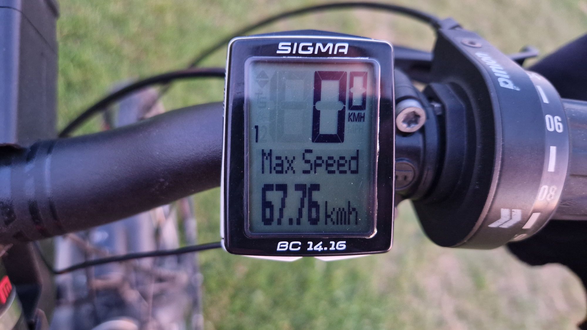
One of the tunnels had an amazing view on the hills and the fjord some 100 meters below. Just a few hundred meters uphill was a viewpoint and a World War II monument, which remembered the “Altmark-drama” at Jøssingfjord in early 1940. I’ve met fellow cyclists from Switzerland, which were a traveling in the opposite direction. We had a very nice chat about the route and what to expect in the respective direction of travel. I think the descent from that hill was one of my fastest ever: 67 km/h downhill!
View on Åna-SiraDam of the Tellnes mine, disposal of Ilmenite (Titanium-Iron oxide mineral)Reaching the topPreparing for downhill bikingFrom Åna-Sira to Jøssingfjord
The following route wasn’t that steep anymore but still covered with lots of smaller hills as the landscape changed progressively into smaller sized hills.
Road and landscape after Jøssingfjord towards Egersund
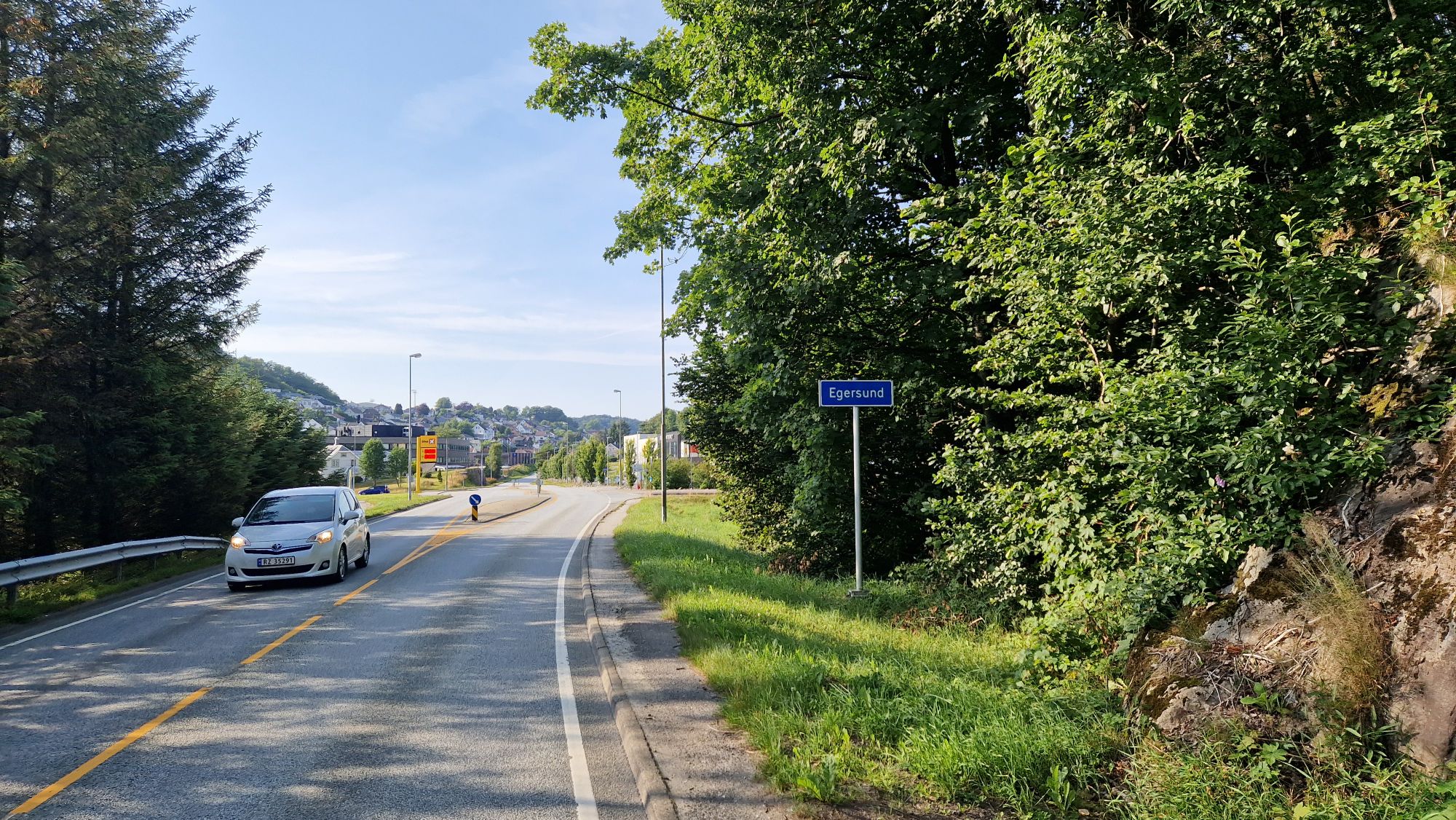
I’ve finally reached Egersund at around 7pm and did some shopping before continuing to Ogna, some 17 km away. The hills were mostly gone but the road changed to gravel-type with annoying steep uphill roads. This slowed me down because I had to push a very heavy bike uphill on a slippery ground. The endless walking uphill gave me blisters.
Finally reached EgersundSteep gravel road after Egersund
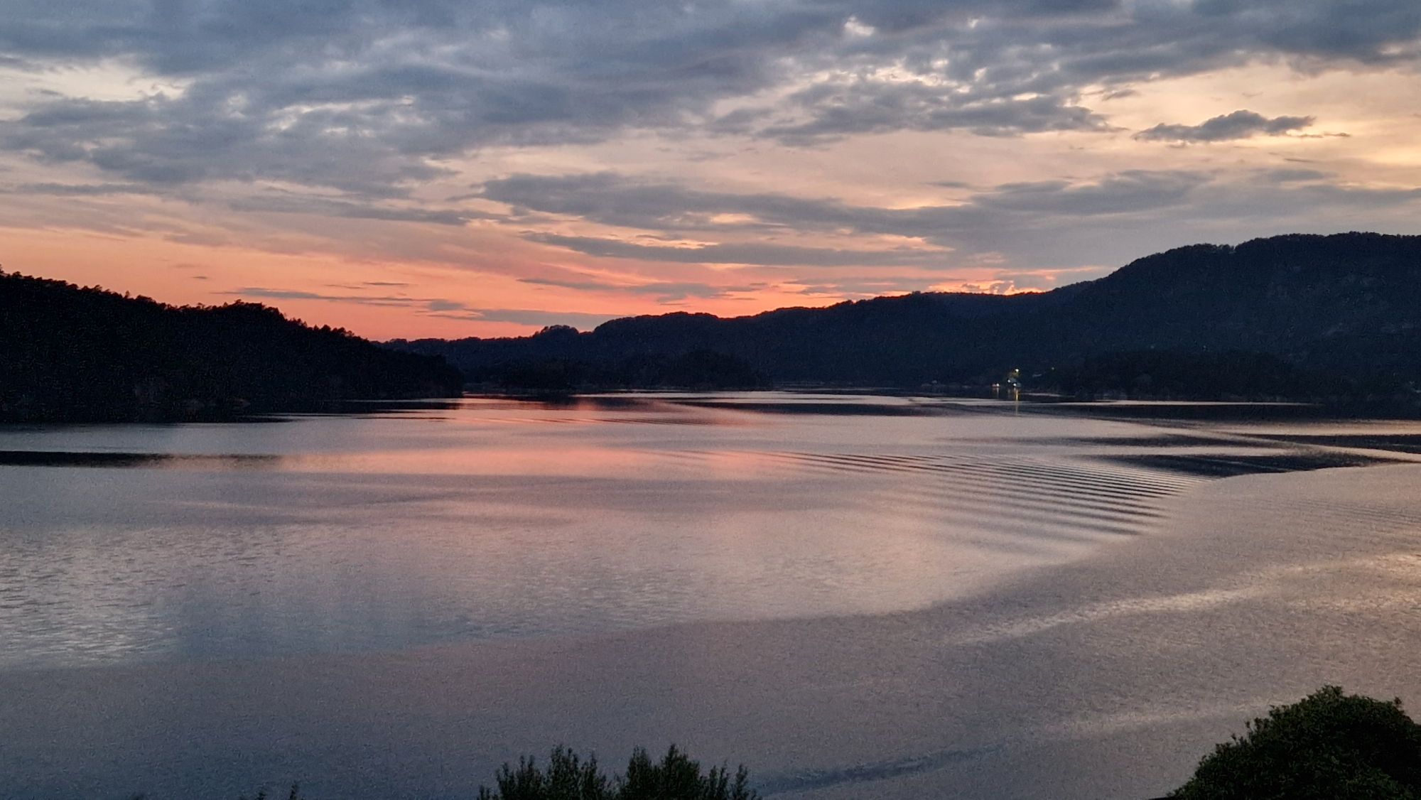
I camped at a local Ogna camping site, close to the beach. I watched the sunset and enjoyed the beautiful views of the sea after a very exhausting but epic traveling day.
Friday, July 11th. Camping at Lomsesanden near Farsund was super nice and affordable. They were very kind and charged my batteries overnight. I moved on at 9:30am and cycled for 10 km just to realize that I’ve missed a Route 1 exit some 3 km ago. So, my route plan needed to be adapted a bit because I didn’t want to cycle back and lose precious time.
Preparing food at the camping siteVisit from a small frogLeaving camping site near Farsund
I went from Vanse to the east in order to get on county road 465. My hope was to avoid the steep hills just like a day before. This worked out well until a tunnel came and I had to take a side road (Ravneheivejen). The side road was very calm with little to no traffic but got very soon, very steep. So I pushed my bike for about 45-60 minutes straight uphill, followed by another 30+ minutes of “ups and downs”. I think the ascent height was 200-250 m. The descendants was very quick with speeds >50 km/h! I really enjoyed this for sure ☺️
My road along the hillsBeautiful views on Farsund
Cycling via county road 465 was fine traffic-wise, but also steep uphill over a couple of kilometers where I had to use low gears at speeds of 6-7 km/h. About 10 km from Kvinesdal, there was another ascent (about 150 m), which took “only” 30 minutes. I met two fellow cyclists from the Netherlands and had a little break and chat with them. Very nice people, they were traveling in the opposite direction and warned me about steep hills to cone. I reached Kvinesdal without any problems.
View on Kvinesdal from top
My last two ascents were from Kvinesdal to Flekkefjord via Feda. Beautiful places! The steep and rocky hills were very impressive. I think pushing the bike was not bad at all because you slow down and see the landscape and nature a bit longer than just passing by. Racing downhill was also rewarding and enjoyable.
Another nice spot near Flekkefjord
I reached Flekkefjord around 8pm and did some shopping and looked out for a toilet and camping. There is a free-of-charge parking lot for camper vans with a toilet. I found a nearby spot where I could set up my tent and rest.
Cannons in Flekkefjord
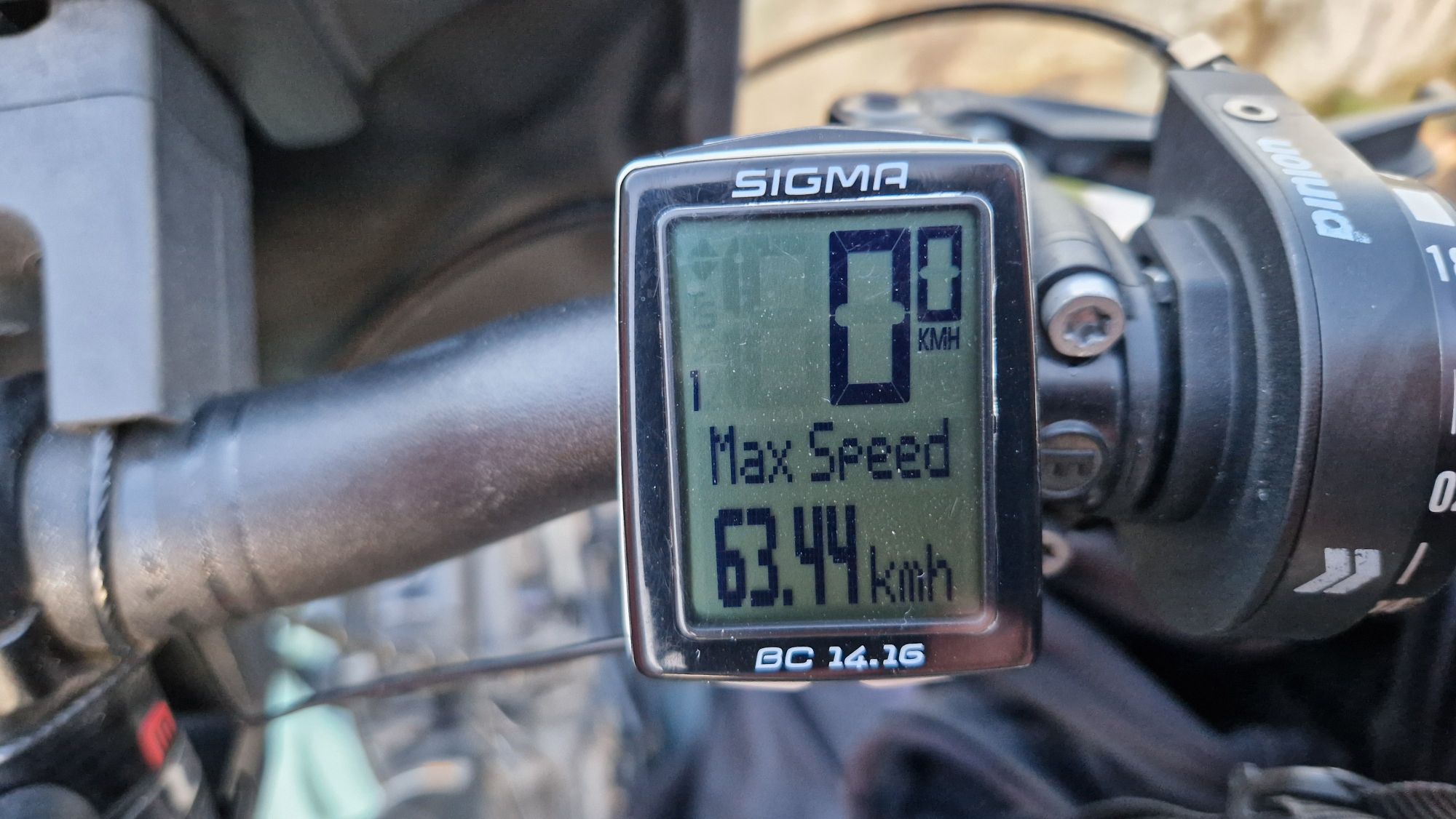
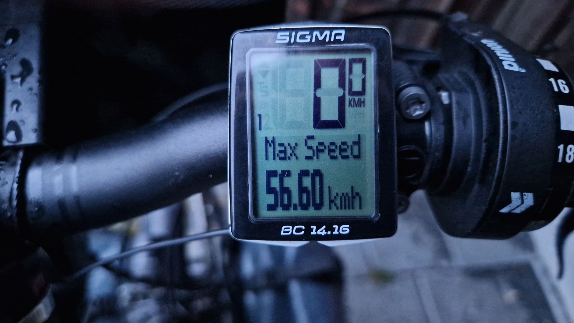
81.62 km, 7h20m, 11.11 km/h, 63.44 km/h (max speed downhill)
Thursday, July 10th. Yesterday’s long cycling day had a huge impact on today’s performance. I didn’t get enough rest and struggled a bit with the time schedule. Everything got a bit delayed, even my daily routine.
My camping spot……well hidden
The day started with very friendly weather conditions (sunshine, 26 °C, no wind). Cycling was very enjoyable and I reached Vigeland and Spangereid quickly.
Statue of an angry guy near SpangereidNaked people all over the places, near Spangereid
Unfortunately, I had to skip my trip to Lydnesnes Fyr, a lighthouse in the south, to keep up with my time schedule. Instead, I tried my first ascend to a steep hill.
This steep ascend near Spangereid was extremely exhausting
This hill was really difficult to climb. From Spangereid to Lyngdal (about 12 km), it took me about 2 hours of bike pushing uphill. Cycling downhill was very nice and fast and took just a few minutes compared to the hour-long ascend. The slope was steep around 15%.
Beautiful views of the landscapeFarsund houses
My legs started to hurt, and after my arrival in Lyngdal, I decided to skip the second ascend and take a coastal route, which was much easier but also with great views on the fjord-like landscapes. I arrived in Farsund with some difficulties (exhausted legs) and set my tent on a local camping site (300 NOK) where I could charge my batteries and have a shower.
Wednesday, July 9th. The stay overnight at Lillesand was great! I could get enough sleep and got amazing views of the landscape early in the morning from top of the 100-meter hill.
Amazing views from top of the hill
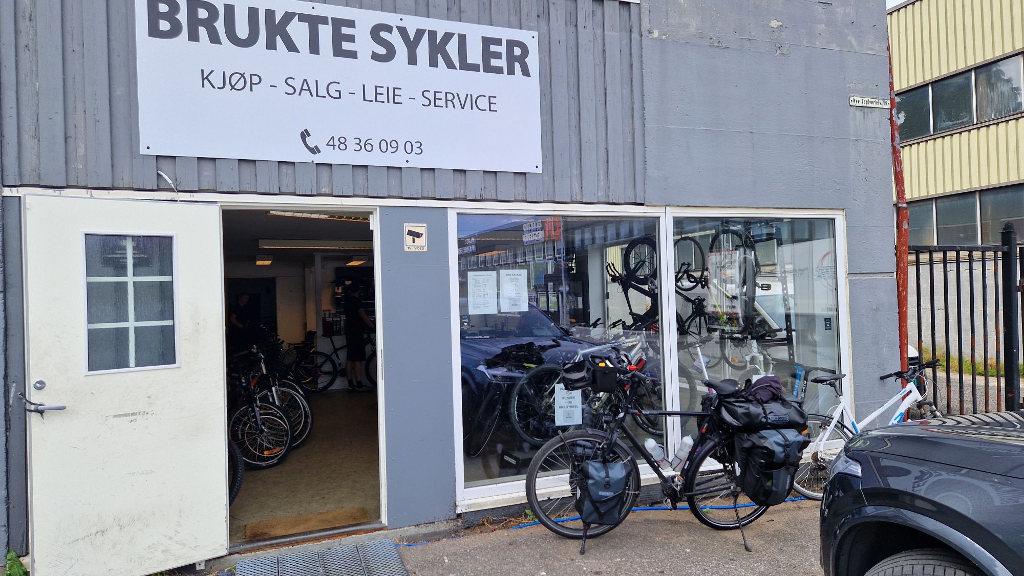
I moved on, and thanks to the mostly flat terrain, my average speed was very good. I passed Birkeland and cycled towards Kristiansand. About 10 km from Kristiansand, I got a flat tire – again. I decided to exchange the hose instead of patching it. A close inspection of the tire revealed small and sharp stones inside of a rubber crack. The tire was damaged from gravel roads and a heavy loaded bike.
Example of a very good bike roadOn the bridge, views towards Kristiansand
After 40 minutes of repair session on a parking lot, I was ready to continue my route and decided to replace the tire in Kristiansand. I spent some time there looking for bike workshops. This cost me a lot of time and my destination city of Mandal was still 60 km away.
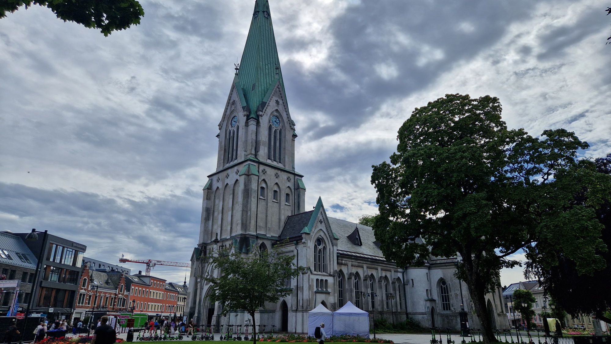
Brukte Sykler Bike shop in Kristiansand, they helped me a lotA church in Kristiansand
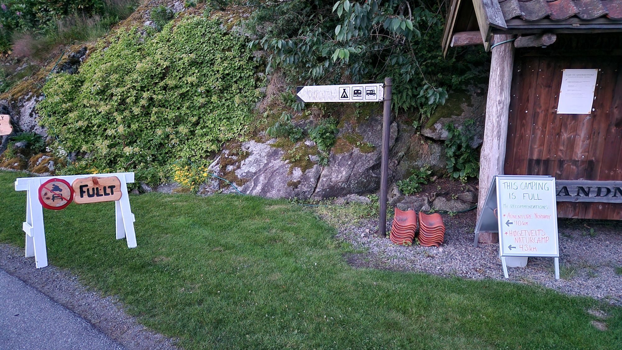
I arrived very late in Mandal around 10:30pm. The local camping site was “full” and no shelter could be found in the city’s proximity. So I had to find a sleeping place quickly, otherwise I’d been in huge trouble.
Mandal camping site was full that evening, thanks for the suggestions for next camping sites – but no thanksMandal promenade by night
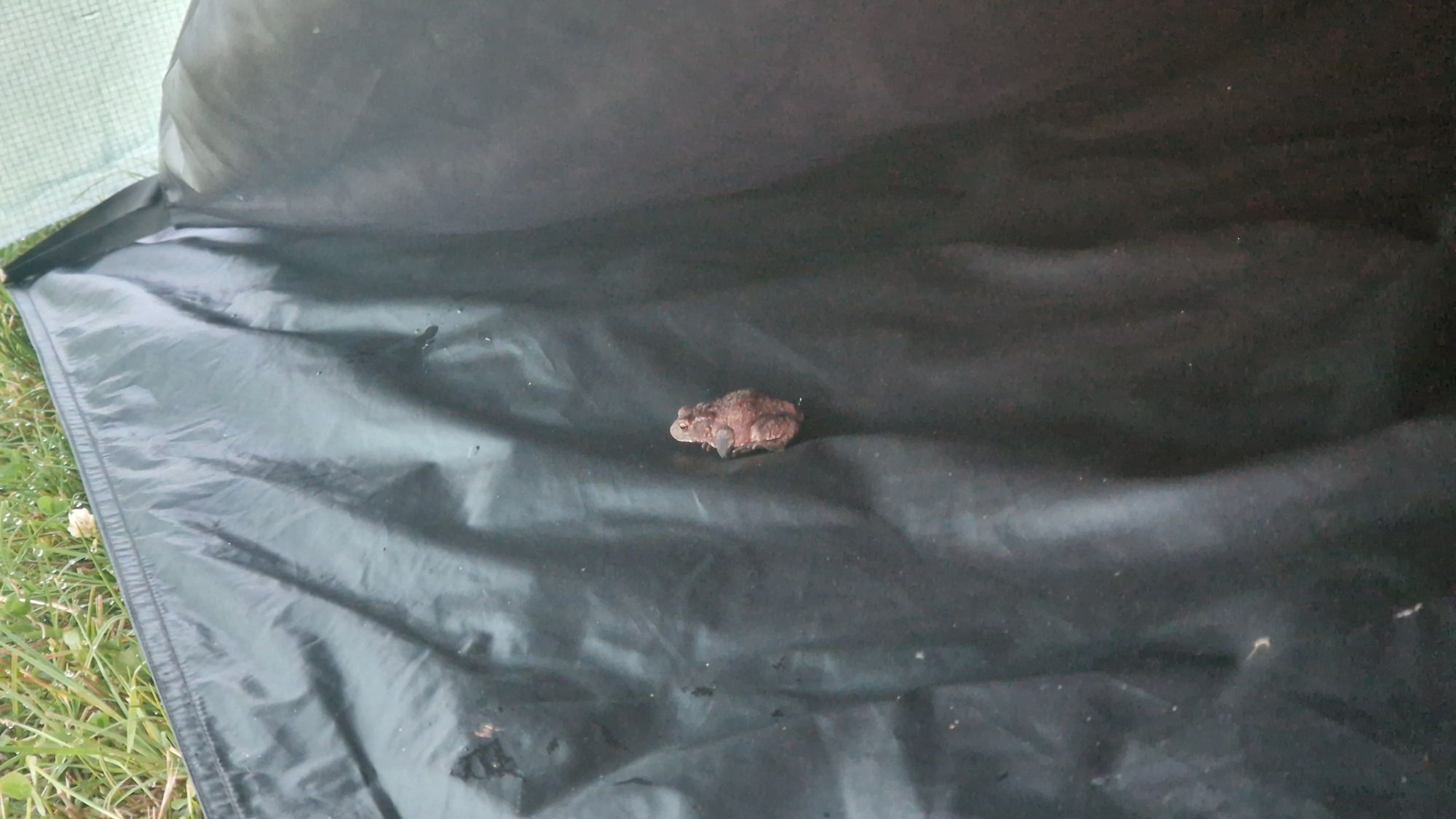
After riding for an hour in complete darkness, around 1am, I found a small place near my road where it had just enough space to put my tent and hide the bike safely. So I spent the night there. I tried to be careful with “blind passengers” when camping in the wild – keeping the pannier bags closed as much as possible and opening the tent zippers for very short periods. Luckily, I found a peck in my tent before she could bite me 😅
My sleeping place that night, setting up the tent in the dark
Tuesday, July 8th. This day was really long and intense. I had a bad night at the shelter and did not get enough sleep. It was raining for 4 hours until 3am. I managed to get back on the road around 7am and stopped a few times for “reasons” (toilet). The weather calmed down at around 16 °C and it stopped raining.
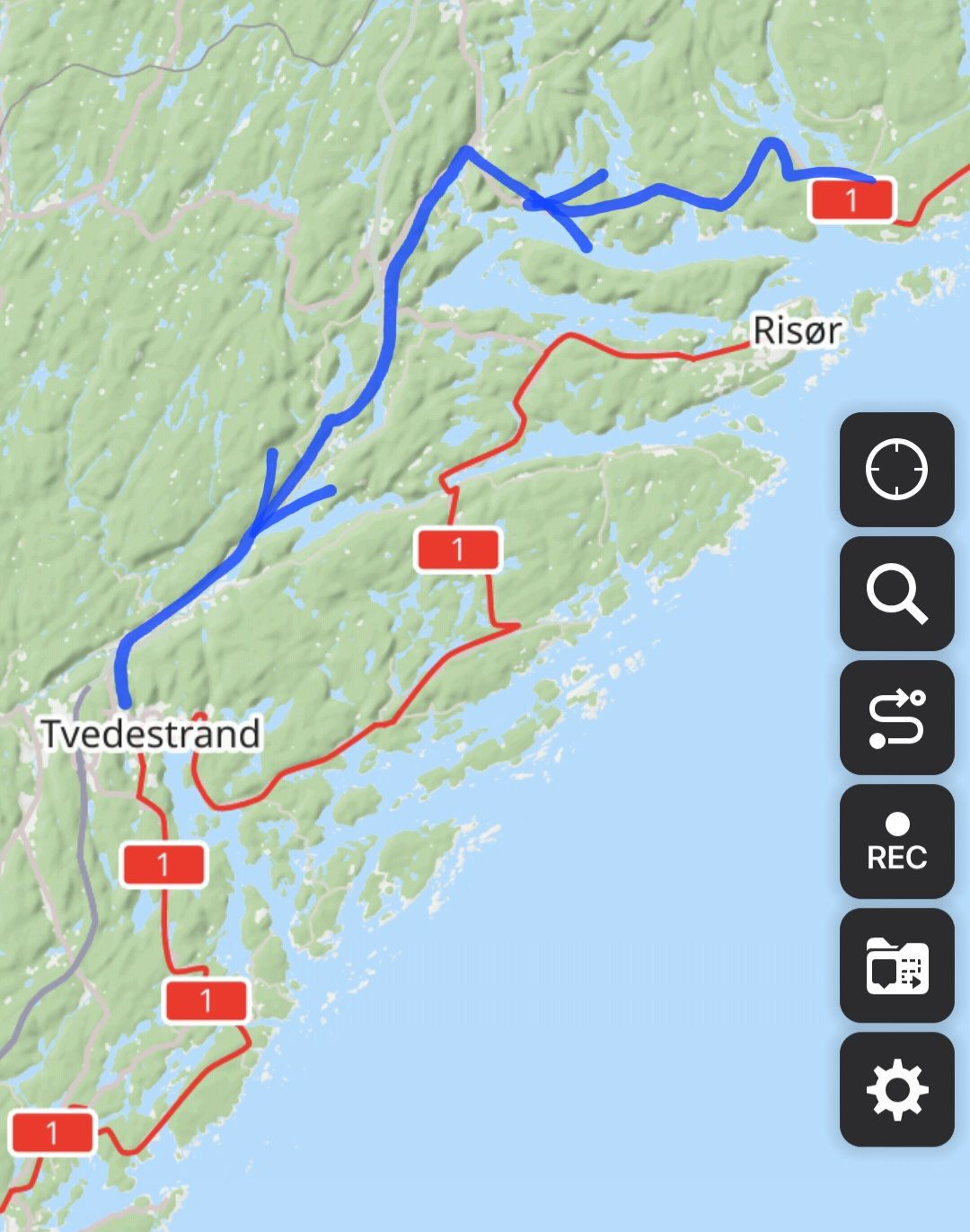
Bad weather during night timeAlternative route (blue)One of the roads from Øysang to TvedestrandBeautiful views on one of countless lakes
I didn’t want to wait a few more hours for the ferry, so I planned an alternative route. The route was similar to the previous days: hills, hills, and more hills… Being tired and not getting enough sleep deteriorated my performance significantly. I had to take breaks just to be able to continue riding. At a certain point, my route app guided me through a forest with gravely roads and steep hills. This slowed me down, and riding through gravel got me a flat tire. God dammit! Sharp stones punctured the tire while riding a heavy bike. The repair went well but cost me another 40 minutes.
Flat tire stopped me in the forestPunctured hose
I’ve reached Tvedestrand at noon, and all of my time advantages by starting early in the morning were gone. The road to Arendal was very exhausting, albeit having the best weather and nice landscapes (did I mention hills?) 😁
Road to Arendal. Someone hanged his shoes on the high-voltage line
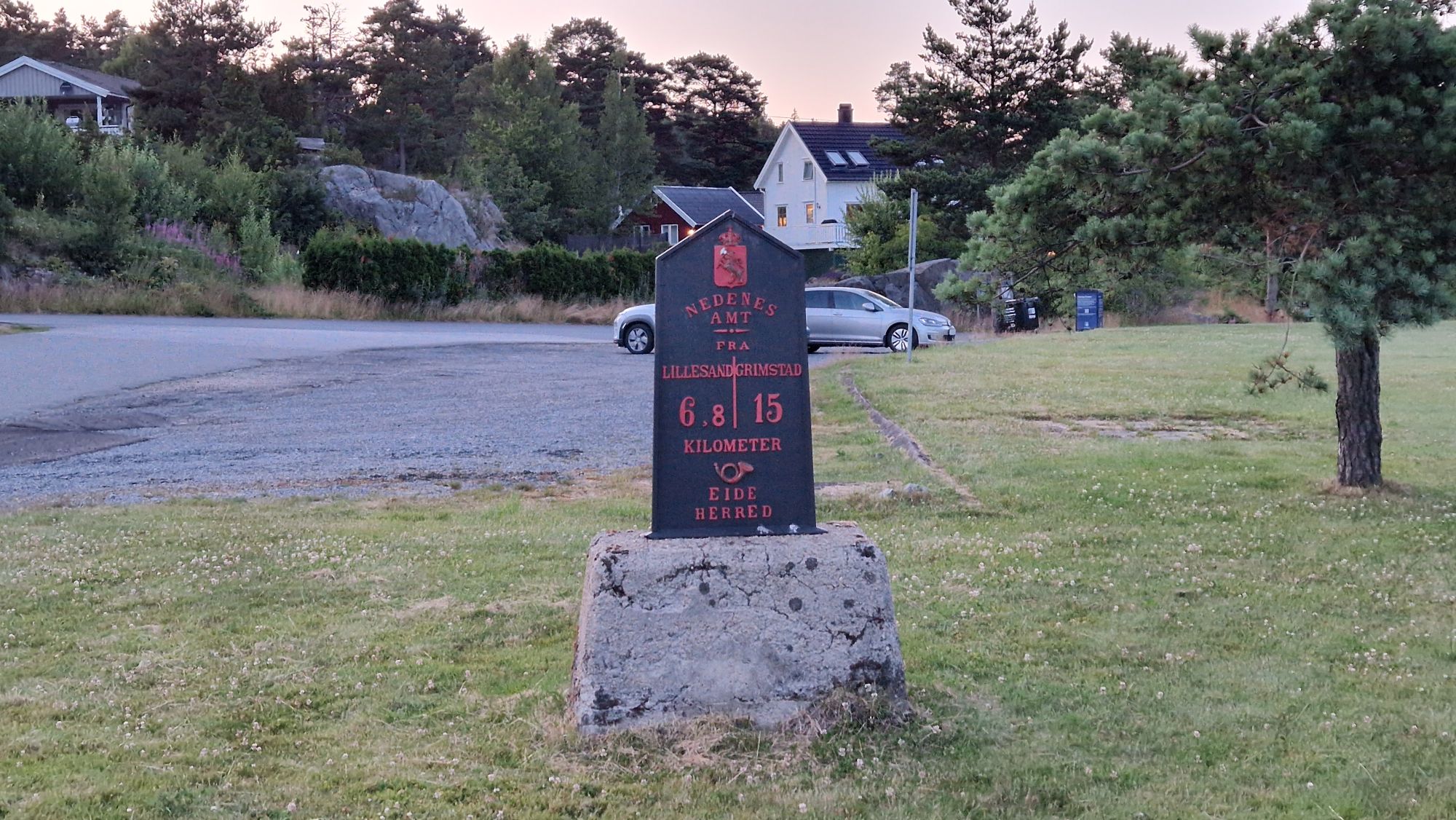
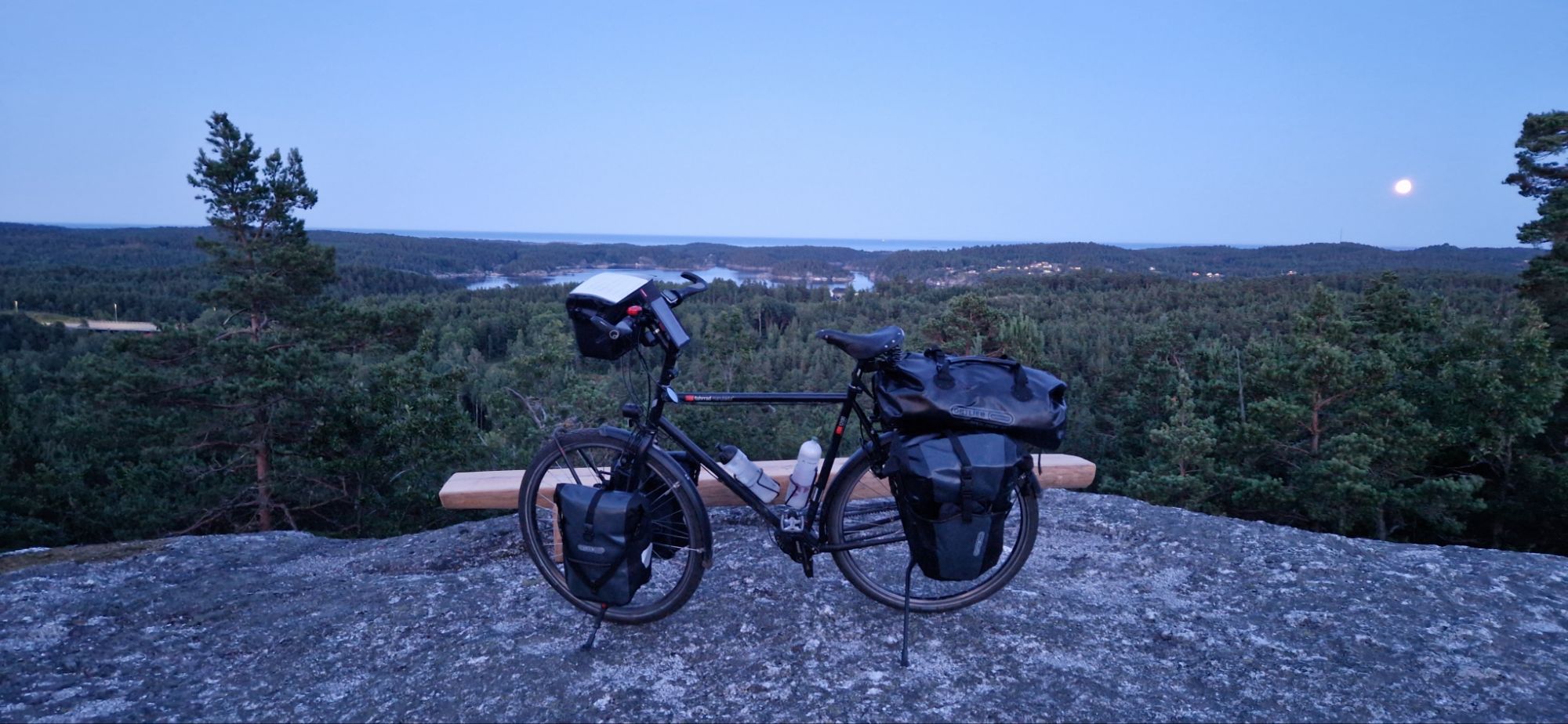
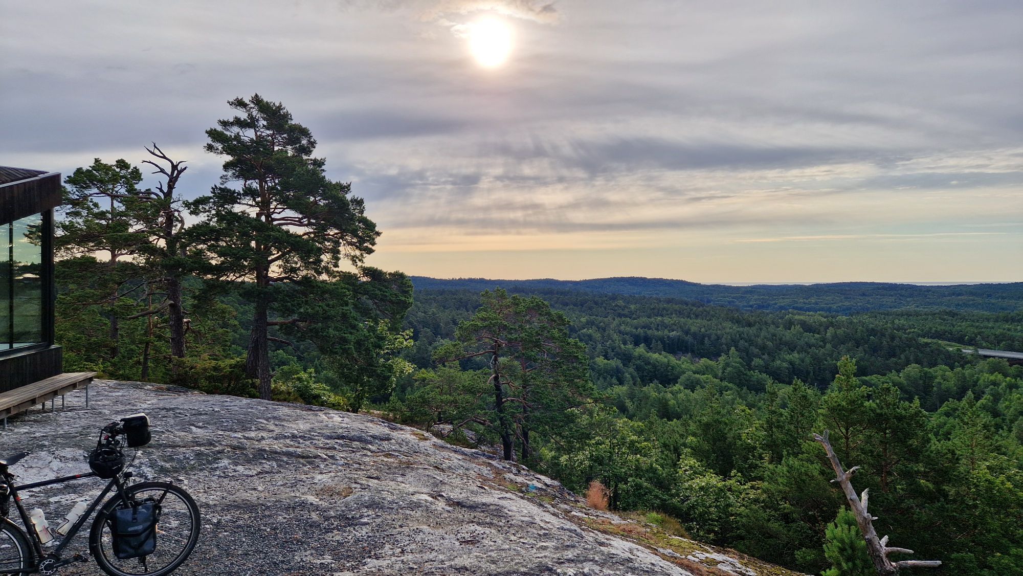
I’ve visited Arendal (wonderful city, met a cyclist from Hannover there) at around 6pm and continued cycling to Grimstad and finally reaching Lillesand at 10:30pm. My app suggested a shelter place near Lillesand. However, it was located on top of a 100-meter high hill. So I pushed my bike uphill late at night – luckily, there was a gravel road. Once standing on top of that hill, I was rewarded with amazing views of the landscape during dusk time. That was worth it. I stayed at the hut that night, albeit it was not allowed to sleep there 😑 That was a small emergency situation, and I did not disturb anyone or anything…
Entering Lillesand in 6.8 kmViews on top of the hillAmazing view next morning
Monday, July 7th. I slept very well in the shelter and did my routine before leaving at 9am. The weather was very good for cycling (overcast, 17-18 °C). The shelter place was a bit hidden in a forest, so it took me about 15 minutes to get back on the route.
Pushing the bike back to the Route 1
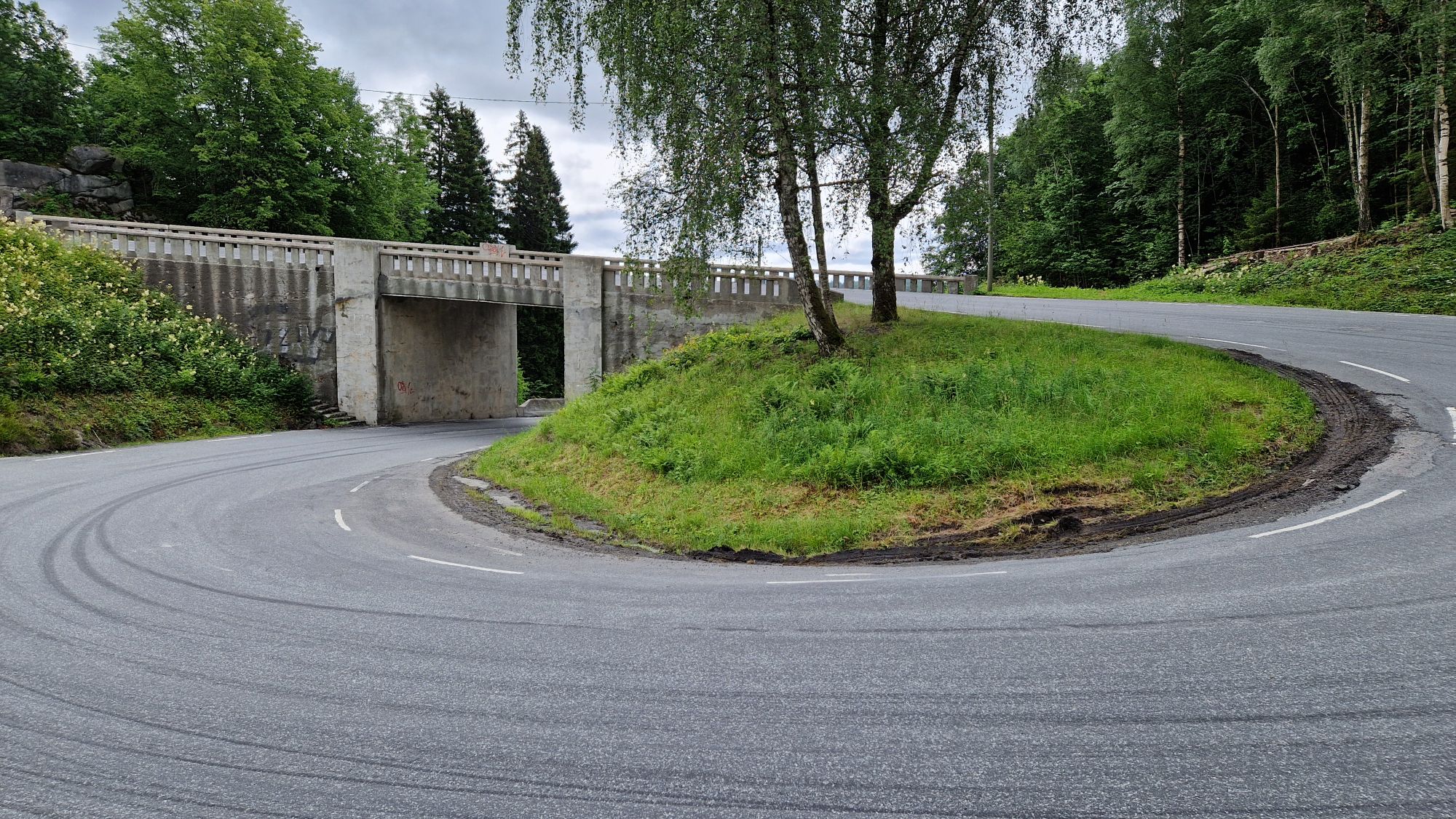
I cycled towards Eidanger near Porsgrunn and continued to Langesund. At this point, the roads revealed their true Norwegian face (as expected): endless hills with forests and massive rocks. My bike is a bit too heavy due to carrying food, water and some unnecessary stuff. So this little inconvenience forced me many times to push the bike uphill while the descend was super nice with max. speeds over 55 km/h! There were also some masive construction sites on the roads, very impressive stuff!
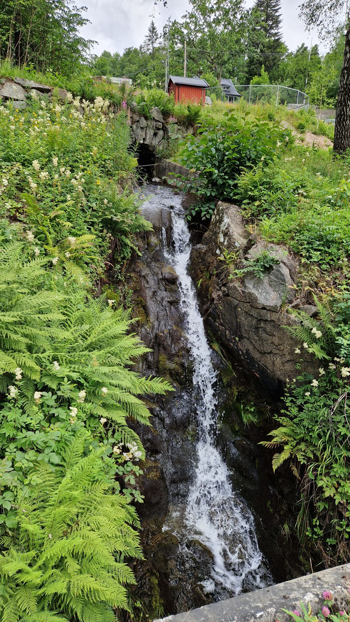
Cycling uphill in a spiral fashionSmall waterfall at the side of the roadOne of the encountered construction sitesLarge construction site near EidangerFrom Nevlunghavn to Eidanger
The route between Langesund and my next destination point in Kragerø was very difficult. There was a 3 km track with steep hills in combination with bad gravel road in a forest which forced me to push the bike 80% of the time. Past the forest part, roads were better but did not lack hills 😅
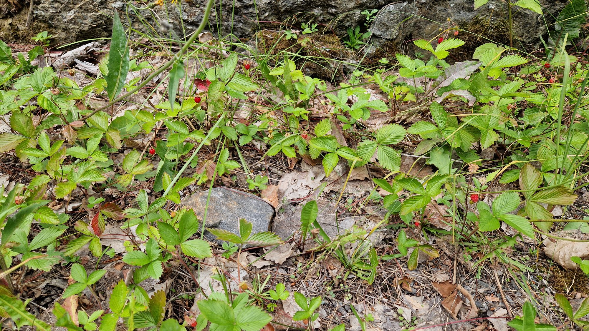
Bridge in BrevikSteep way to the bridge in BrevikView from the Brevik bridgeForest road outside of Langesund. Had to push the bikeVery steep and dangerous downhill roadWild berries (strawberries), growing along the roadsSize of a wild berry is about 5-8 mm in diameter. I saw them growing in Sweden, tooFerry in StabbestadFrom Eidanger to Kragerø/Stabbestad
It took me 5 hours to cycle 40 km of this kind of terrain. In Kragerø I took the ferry to Stabbestad and continued cycling to Øysang, a small village near my destination city of Risør. This part was about 13 km and took me 1.5 hours.
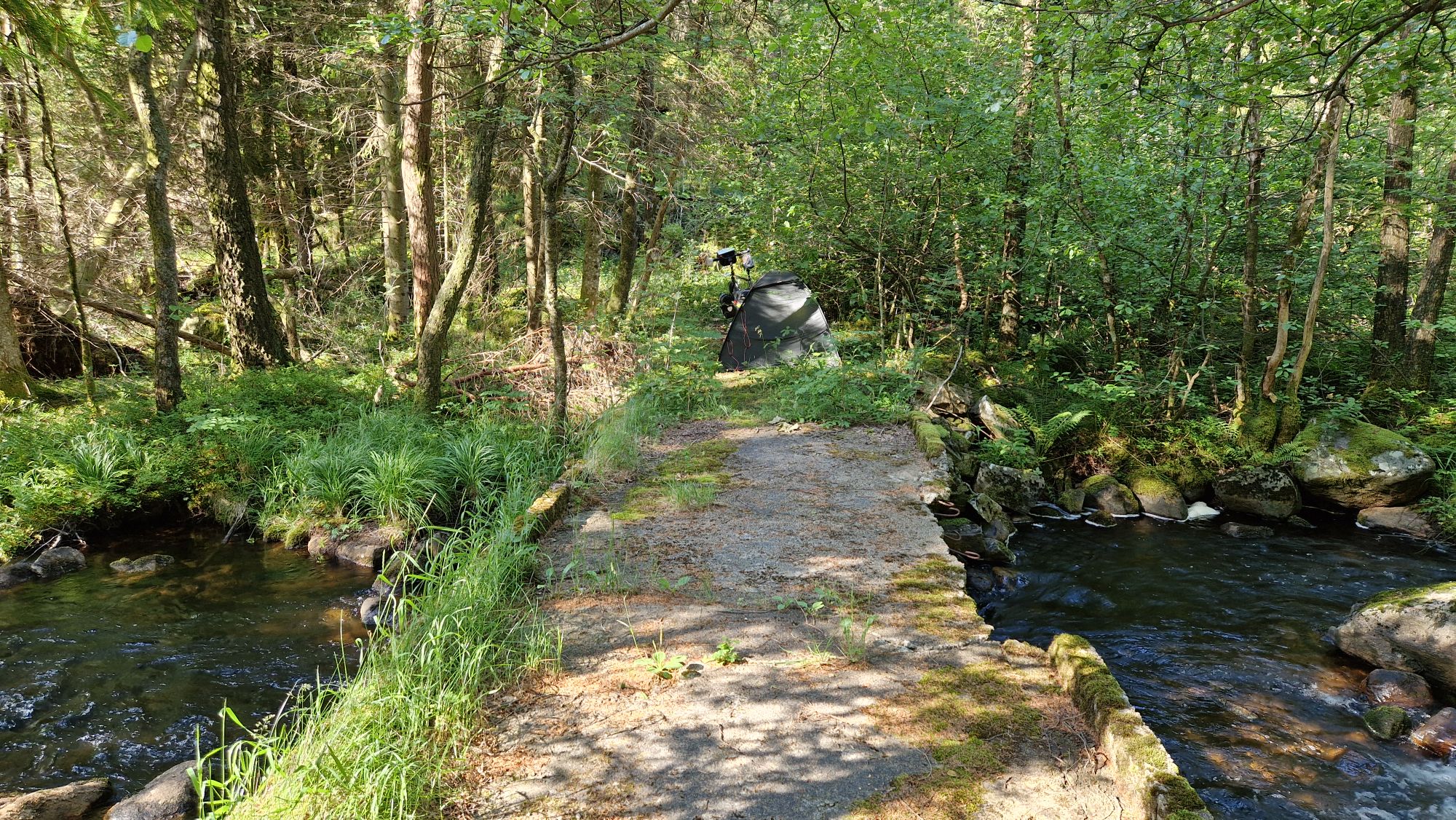
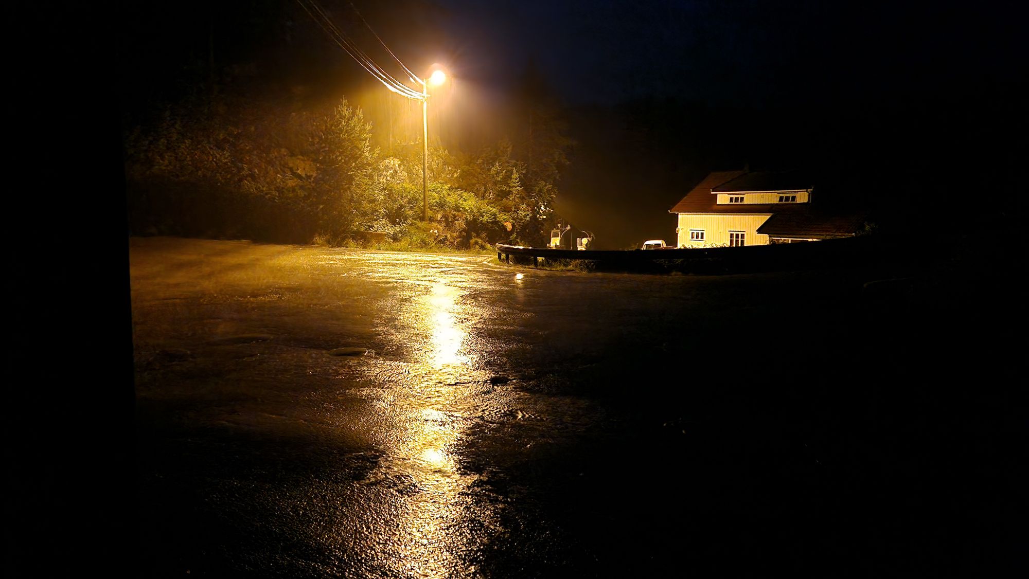
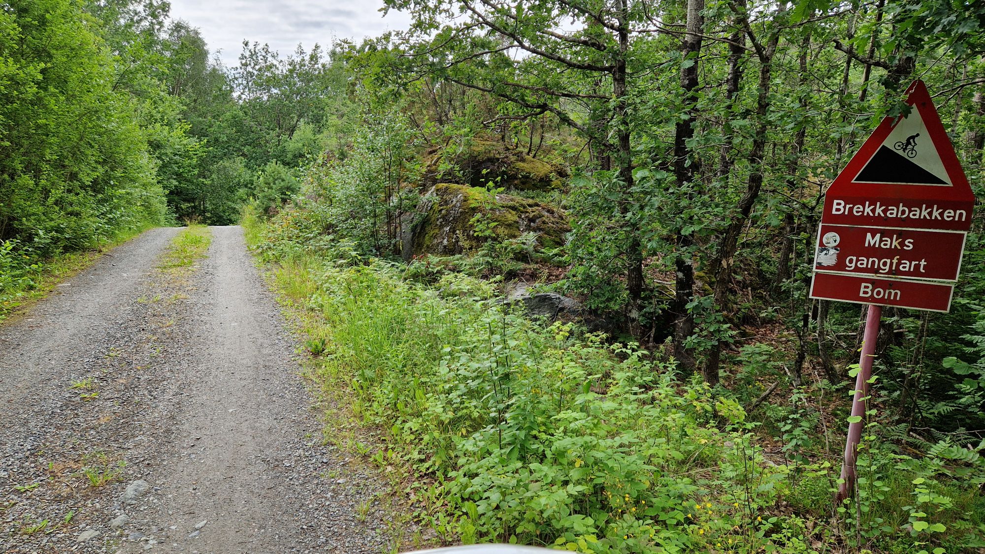
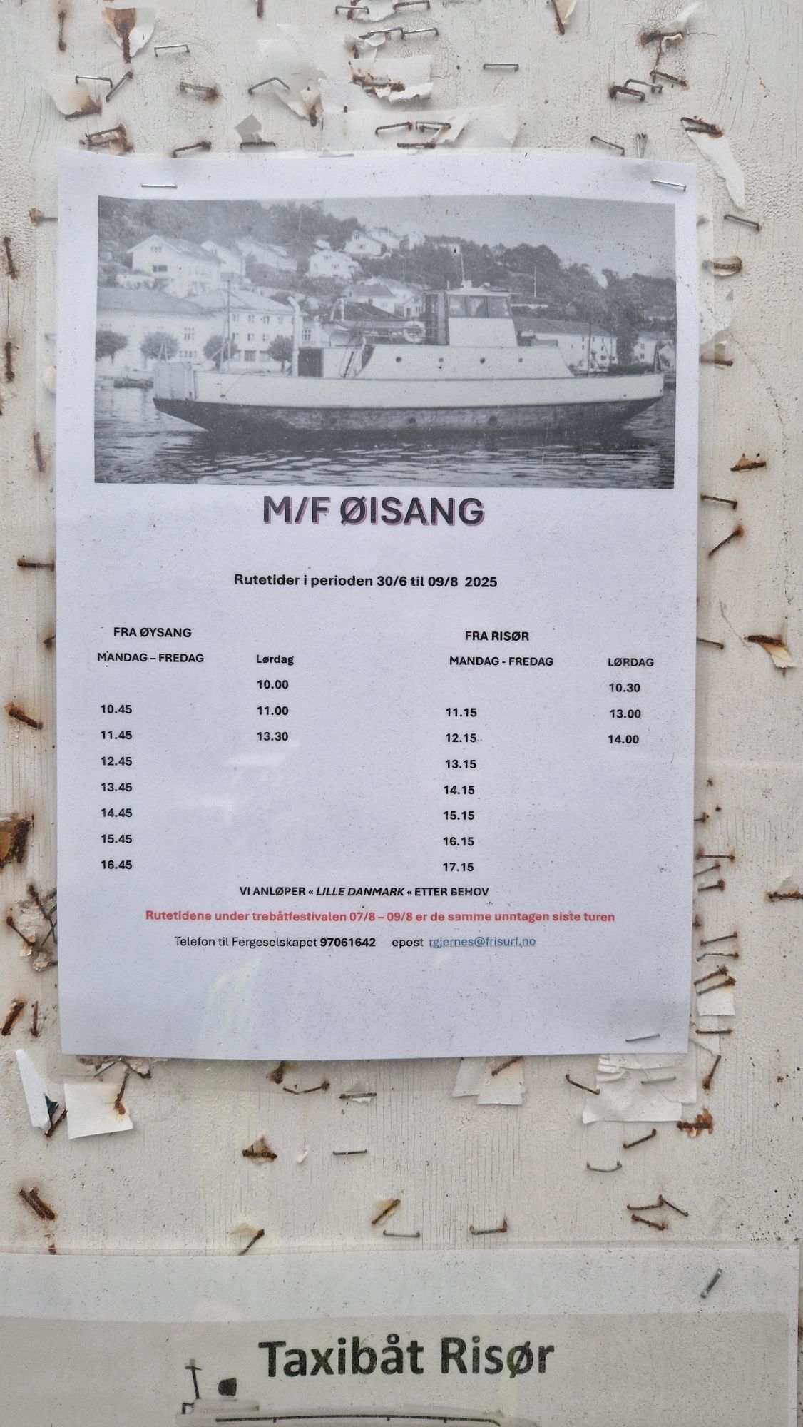
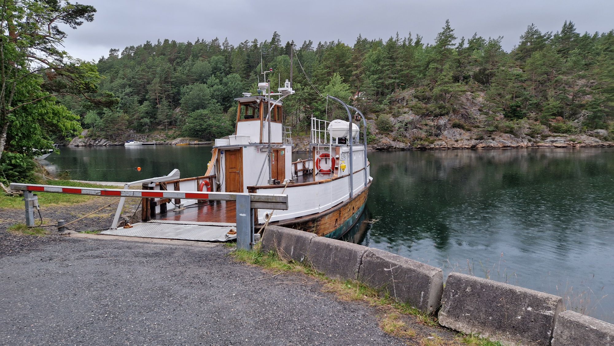
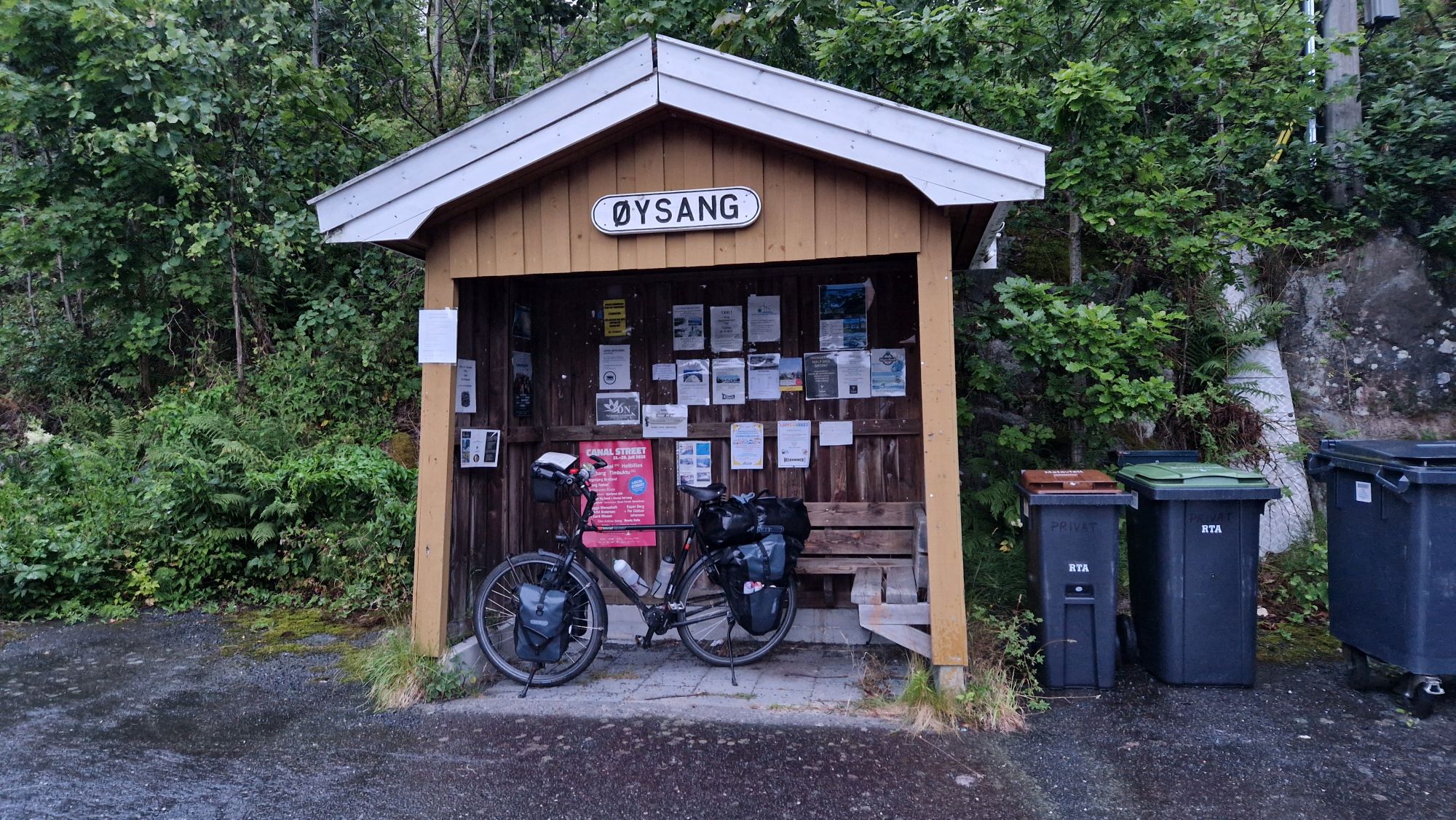
According to my plan, in Øysang should have been another ferry which should take me to Risør. Upon my arrival in the harbor, everything went south: the ferry was closed for this day and it just started raining for the next 5 hours. The next ferry would leave at 10:45am on Tuesday, which is too late for me.
Øysang ferry schedule, “Fra Øysang” means “From Øysang [to Risør]”
After standing some time in the rain and not knowing what to do next, I found a small covered stop with a bench – just to escape the rain. I decided to stay there for the next couple of hours and get some rest and try to move early in the morning. I might skip the Risør ferry and get ahead in schedule if I circumvent the bay. I would return back to Route 1 in Tvedestrand, about 30 km away from Risør.
Øysang ferry, closed for this dayMy “shelter” for this night…god damnit, not again 😩Pissing weather at night
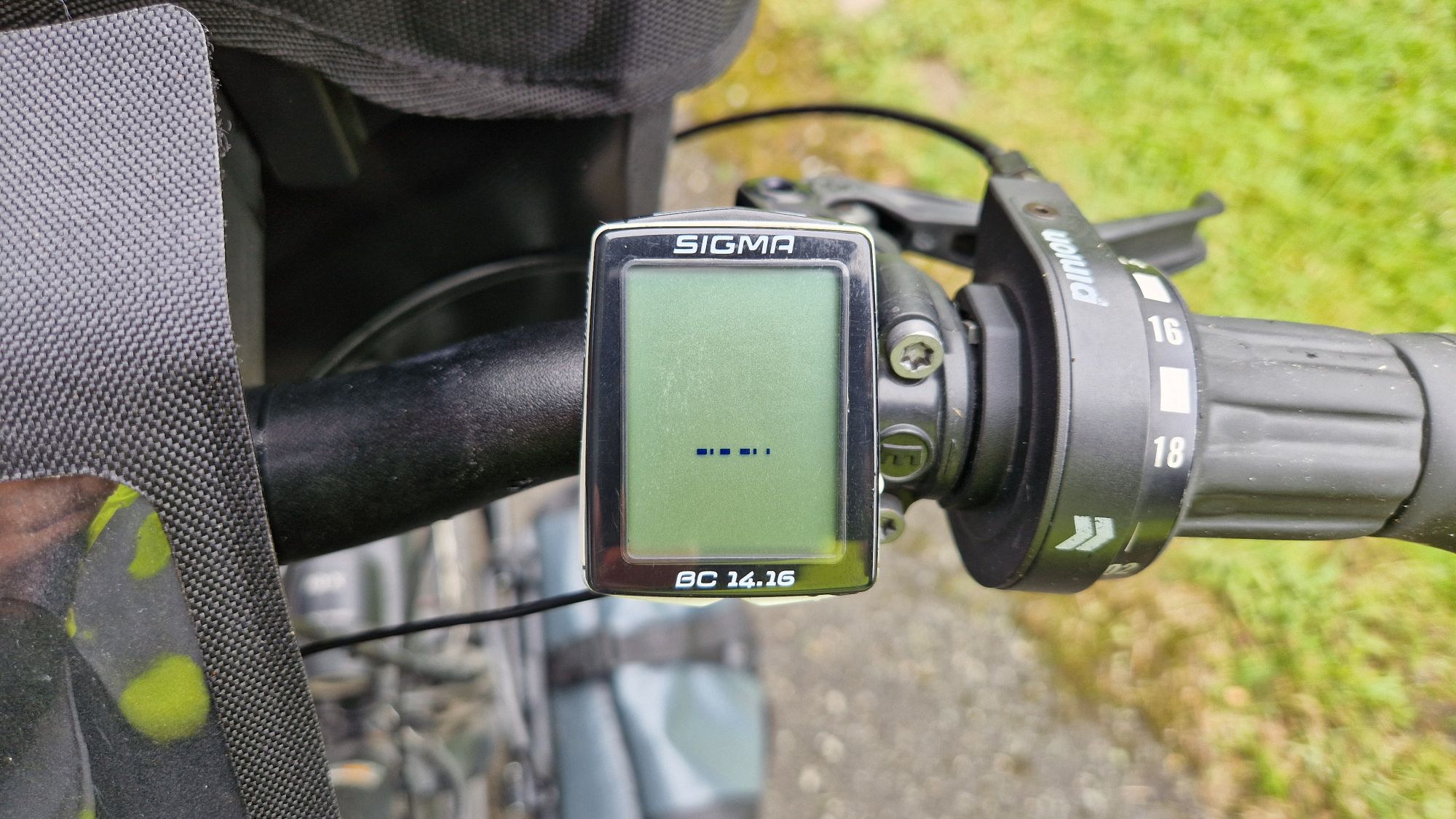
The heat treatment of my bike computer with pocket oven worked very well! No more reboots.
Sunday, July 6th. I had a good sleep and the tent got dry again. I had to change the brake pads due to terrain for the past 1000 km or so. The weather was very nice on this day: sunshine, 21 °C and little to no wind. The roads were great but also full of hills – had to push my bike quite few times uphill.
Serviving the bike, exchanging of the brake pads
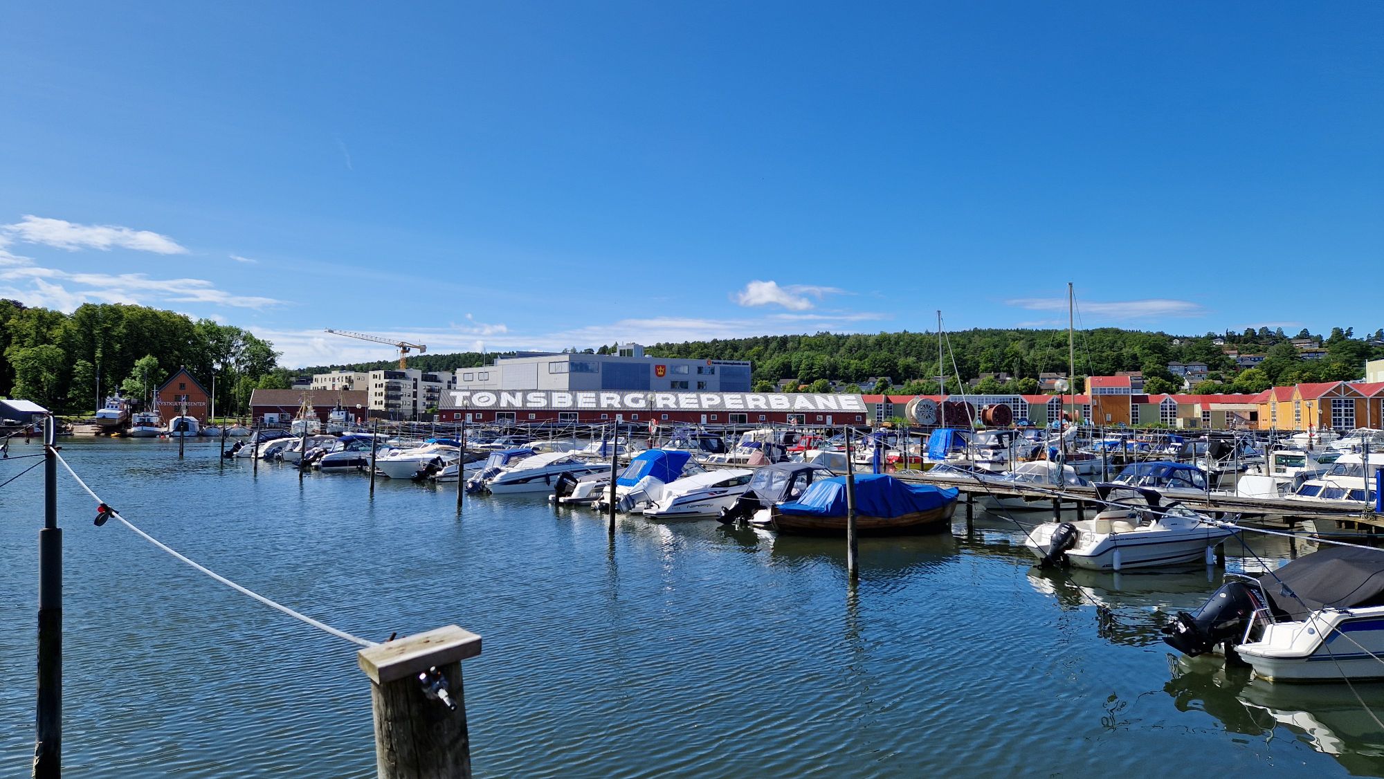
I’ve visited Tønsberg and Sandefjord, both very nice places.
A Reeperbahn in Tønsberg!Steep hill – again….Awesome fountain in Sandefjord, it shows fishermen at whaling
My bike computer showed some life signs during sunshine (heats up, releases some moisture) but it was still rebooting intermittenly. I will try to dry it with a pocket oven. The pocket oven is filled with Zippo lighter gasoline and the gasoline is burnt slowly by a catalyst material over few hours. It releases enough heat to keep things like hands warm at cozy 40-50 °C.
Moisture inside of bike computerPocket oven used for drying 😅
Today’s shelter was hidden near Nevlungshaven. Amazing place near a bay where one could take a bath. I really liked this place and after having a dinner, I went to swim a bit. Perfect ending for a long day.
Tonight’s shelterPlace few meters away from the shelterPanorama view of the bay
The day started at 6am with some low-intensity rain which built up steadily. I packed my stuff inside of the tent and prepared myself for the rainy weather. As soon as I stepped outside, my rain clothes were fine and dealt with rain very well. However, the tent got wet and I had no chance to pack it in a dry place. I left the camp site at 9am and had to navigate to the cycling route while it was raining. Luckily it was mostly cycling downhill so I was able to be on route in about 30 min without difficulties.
My tent (Hilleberg Unna) has an antechamber where I can store my bags in case of raining weather conditions
The next 4 hours were “OK” for cycling – heavy rain but no wind and not to steep terrain. I couldn’t take photos becsuse everything would get wet in few seconds. At a certain point I was wet outside due to rain and also wet inside due to sweat. That’s no problem as long one stays warm. My feet are my weak point 😅 Once they are soaked and cold – game over. But luckily not this time.
Stopped here for a break and tried (unsuccessfully) to clean my tentA park in the city of Drammen where I set up and cleaned the tent
I visited the city of Drammen where I was able to set up the wet tent in a park and remove the water as best as possible. This is extremely important on bike tours – wet tents can be a showstopper. The moisture needs to be removed, otherwise the tent will get “moldy” 2-3 days later. Sleeping in a wet tent is also very uncomfortable. Every time you encounter this situation, stop at a dry place (under a bridge for example) and clean the tent.
The journey on Route 1 continued until it “ended” abrupt near Kjeldås. My way to the city of Horten was mostly via country roads and I had to use smartphone navigation a lot. The weather got better by the evening and I reached Horten without problems.
Incoming ferry from Moss in HortenBack on Route 1
I cycled about 12 km more to a hidden shelter just outside Åsgardstrand. It was located inside of a forest. The shelter place had a hut where I could stay alone for a night. I set up the tent once again, dried it and slept inside (to fend off pesky mosquitoes).
Shelter in a forest few kilometers outside of ÅsgardstrandNo bears attacked me (yet) 😅
My bike computer got wet and it stopped working. Probably some moisture got inside and messed up the electronics. It keeps “rebooting” so no accurate kilometer estimate is possible right now. RIP
Bike computer didn’t survive the rain and keeps rebooting
I cycled around 100 km according to the map measuring tool.
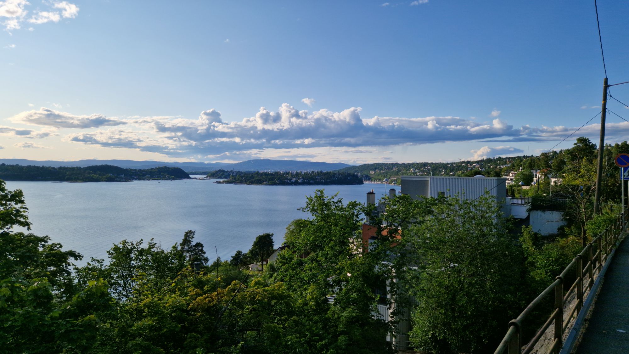
Friday, July 4th. Free day to hang out in Oslo. Weather was superb – sunshine, some 20ish °C, mild breeze. After leaving the camping place and swearing never to visit them again*, I looked for a quiet place in a park to choose some few places to visit. I was carrying a lot of stuff with me so climbing the hills of Oslo was not an option.
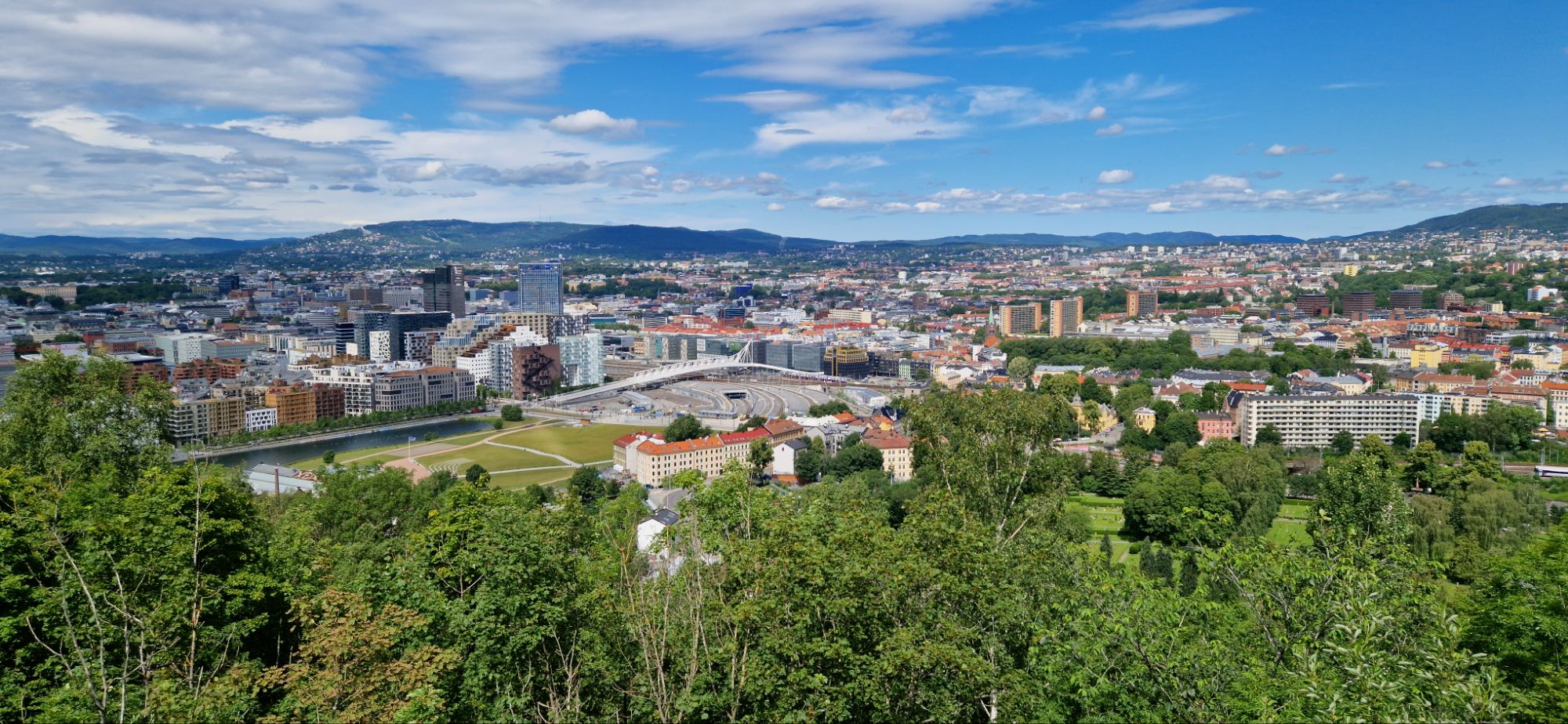
View on Oslo from Ekeberg
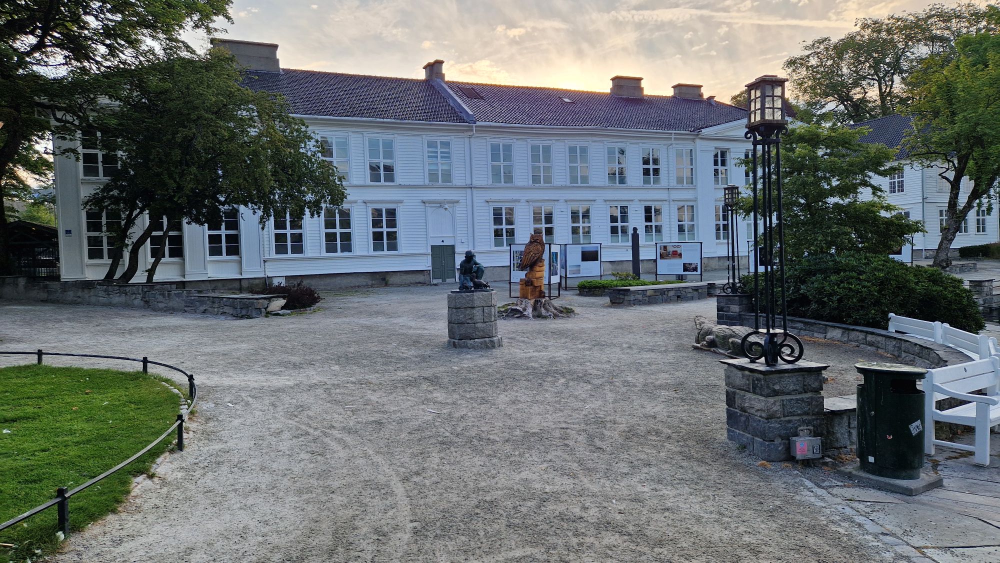
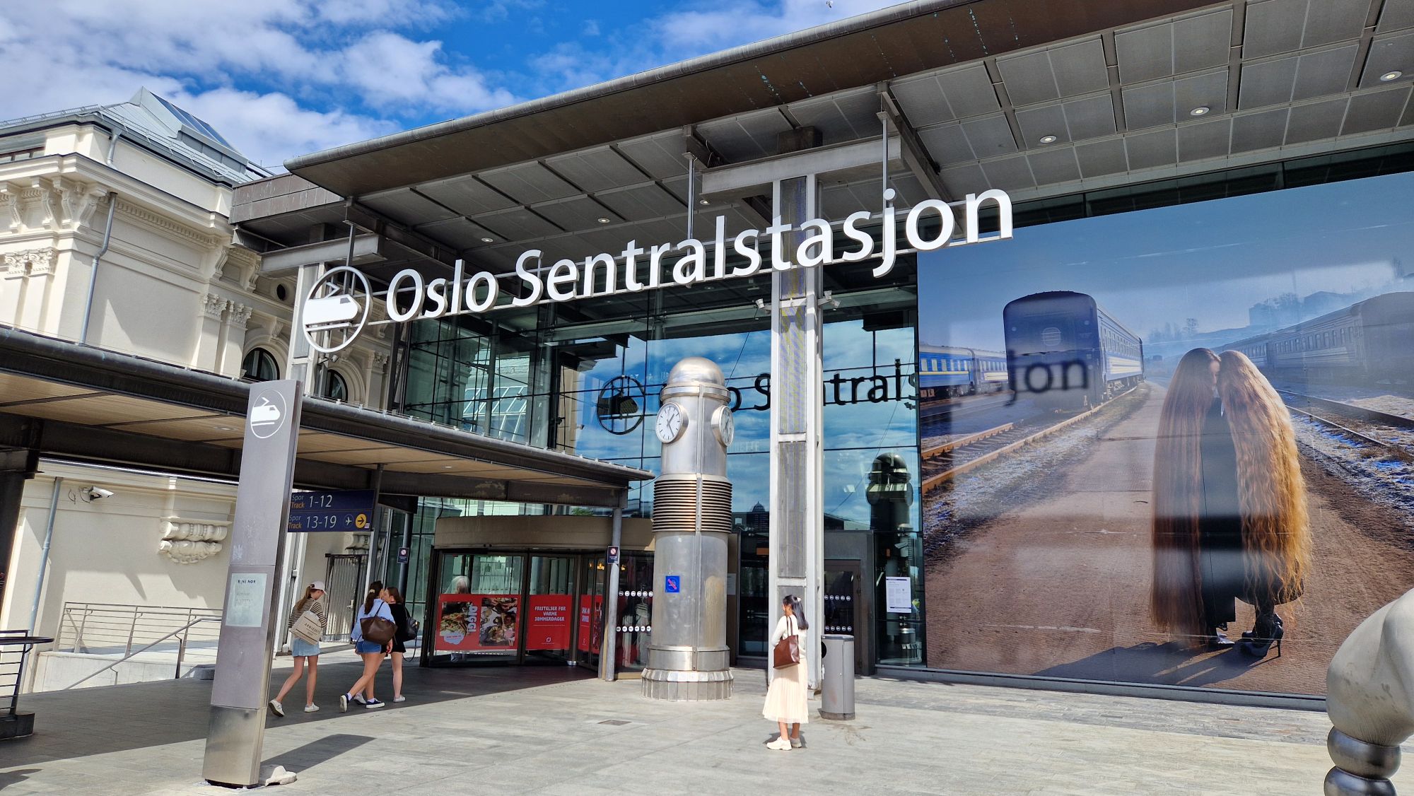
I’ve visited the central station, the opera house, the city hall, the parliament, the cathedral, the Royal Palace and the German embassy. Along the route, I’ve seen the harbor where ships commute between Oslo and Kiel.
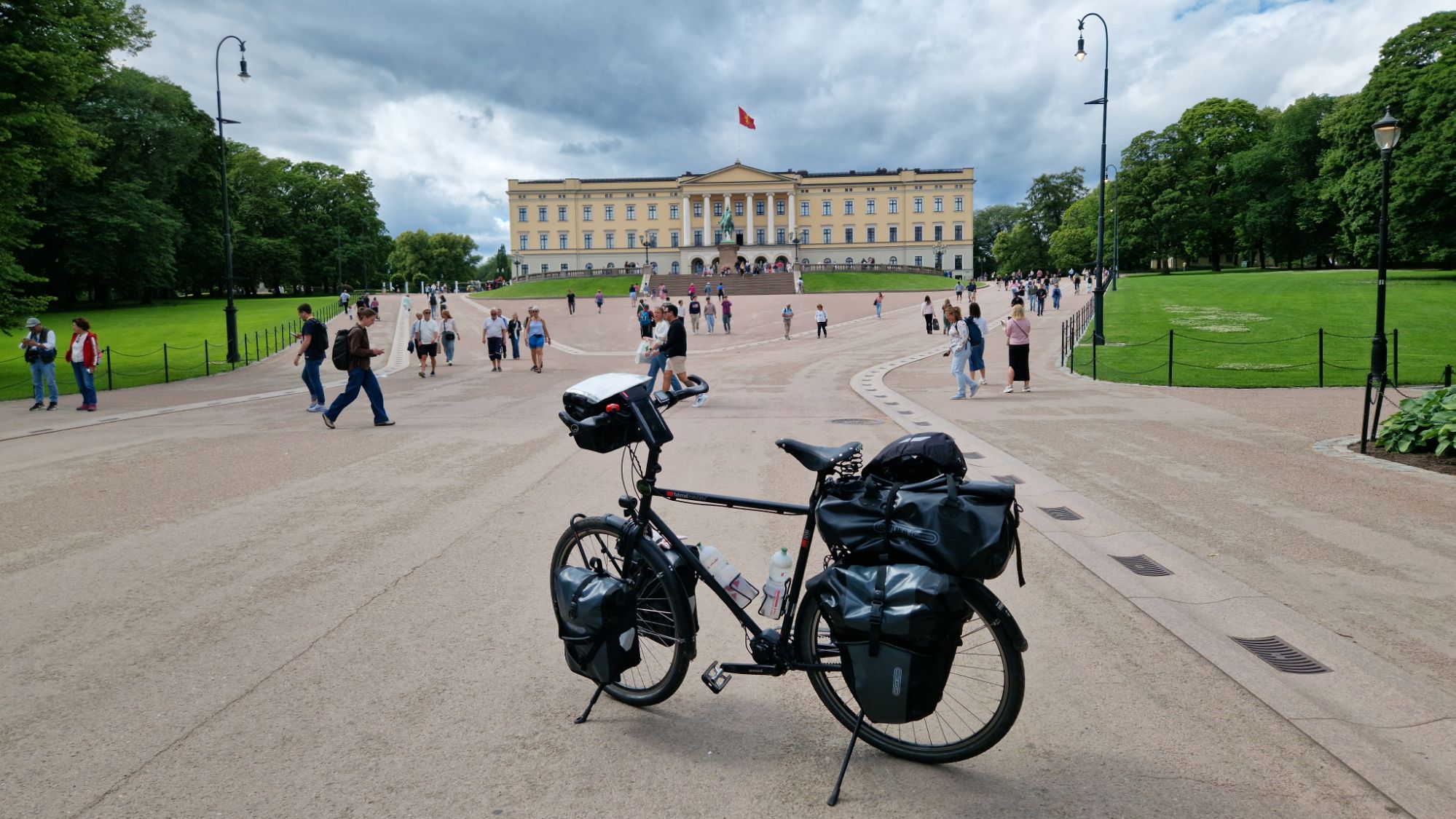
Oslo SNaked people all over the placeBike posing in front of the Royal Palace
In the evening, I thought I’d give another camping site a try. After driving up the hills for 30 minutes, I arrived at another Top Camp site in Oslo. Oh, the horrors – not again… Anyways, paid 50 EUR and I was shocked by the construction site I saw behind the entrance 😅 Luckily, everything was fine: quiet place, well maintained service house – no problems whatsoever. They were very kind to charge my batteries over night.
Construction site behind the entrance of the camping site
I talked to nearby campers about my journey and they gave me some useful advices for my future travels to eastern/northern Norway! Great day with some rainy clouds on the horizon.
Not many kilometers today… 24.9 km, 7.8 km/h (mostly walking through the city and climbing the hills)
Thursday, July 3rd. Day started with pissing rain at 16 °C. I felt no hurry to rush things and had some coffee and snacks. The sleep in the shelter was excellent besides mosquitoes waking me up during the night.
“Morning chaos”
The tour started a bit late at 10:30am. It was raining on and off for an hour but the weather got better by noon. The first 10 km on the roads were nice and quiet until I approached larger cities where traffic noise dominated the background noise.
Some “gems” picked up along the way. I like this
Reaching Moss was pretty much straight-forward, however, I got slowed down significantly by construction sites spread over multiple towns. Some parts of the route were closed, so finding alternative routes cost me some additional time getting back on route. Navigating through cities in a zig-zag manner was hell. I lost the way many times and finding back on route was very time-consuming.
One of the construction sitesYep… My mindset on this day
Anyways, at a certain point I ignored everything around me and just wanted to get to Oslo as fast as possible in order to escape the “Göteborg fiasco” as described few days ago…
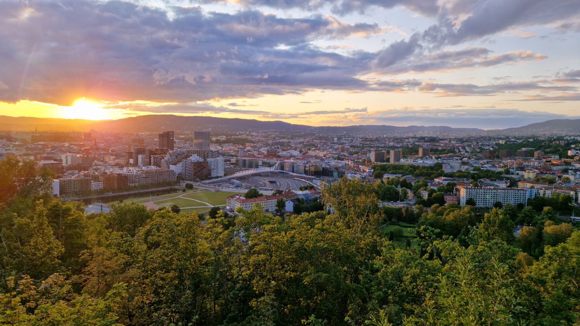
I approached Oslo around 8pm. I had a view from the hills descending towards Ljan. The evening sun was shining and it was beautiful. Every 100 meters I had to take new pictures because more details appeared.
View on Oslo
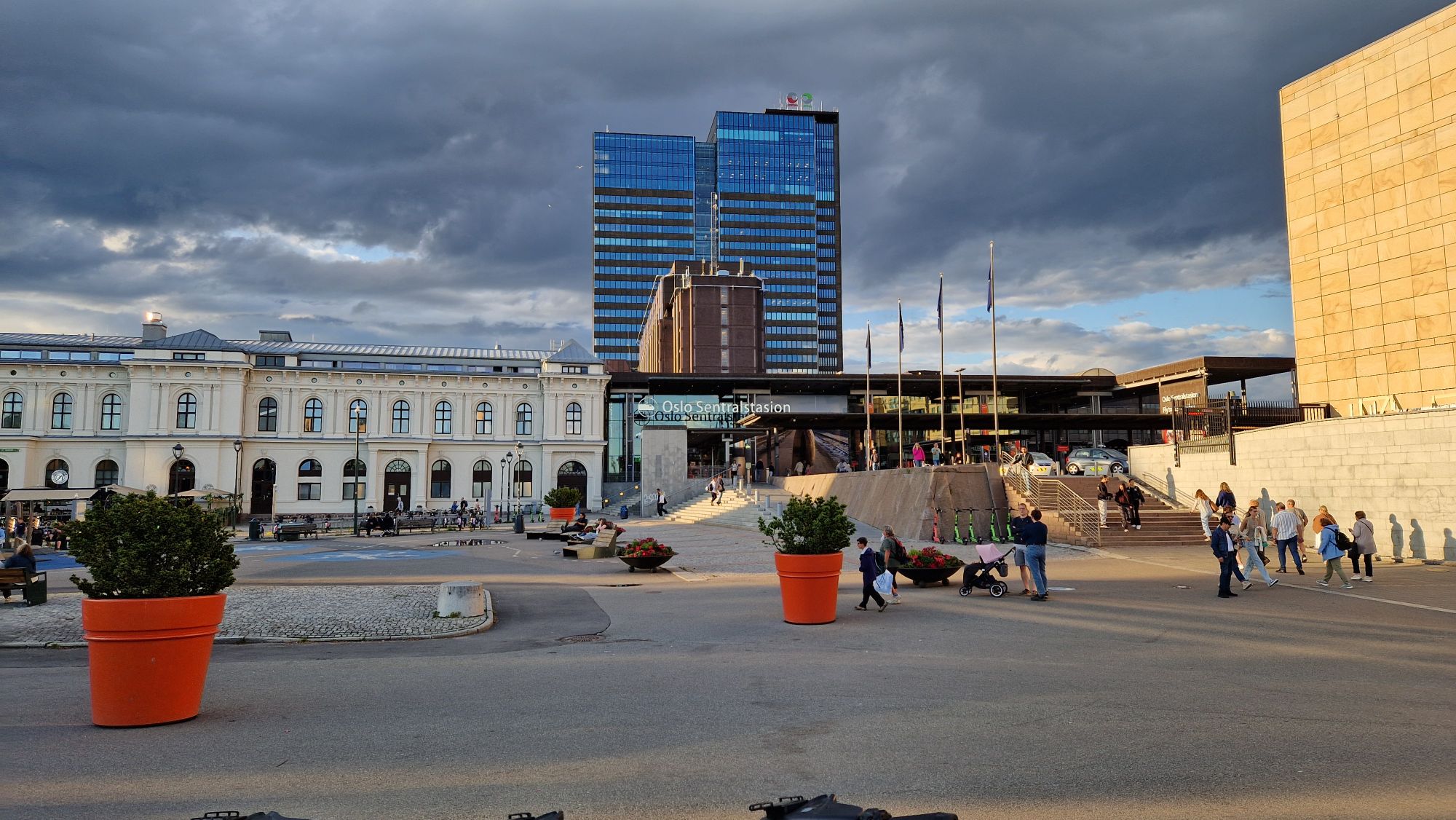
The descend showed some issues with Oslo: lots of traffic, little parking space, many private properties, small sidewalks (barely enough space for a pedestrian). I visited the central station Oslo S prior to moving to a camping site in Ekeberg.
There we are! Oslo Sentralstasion
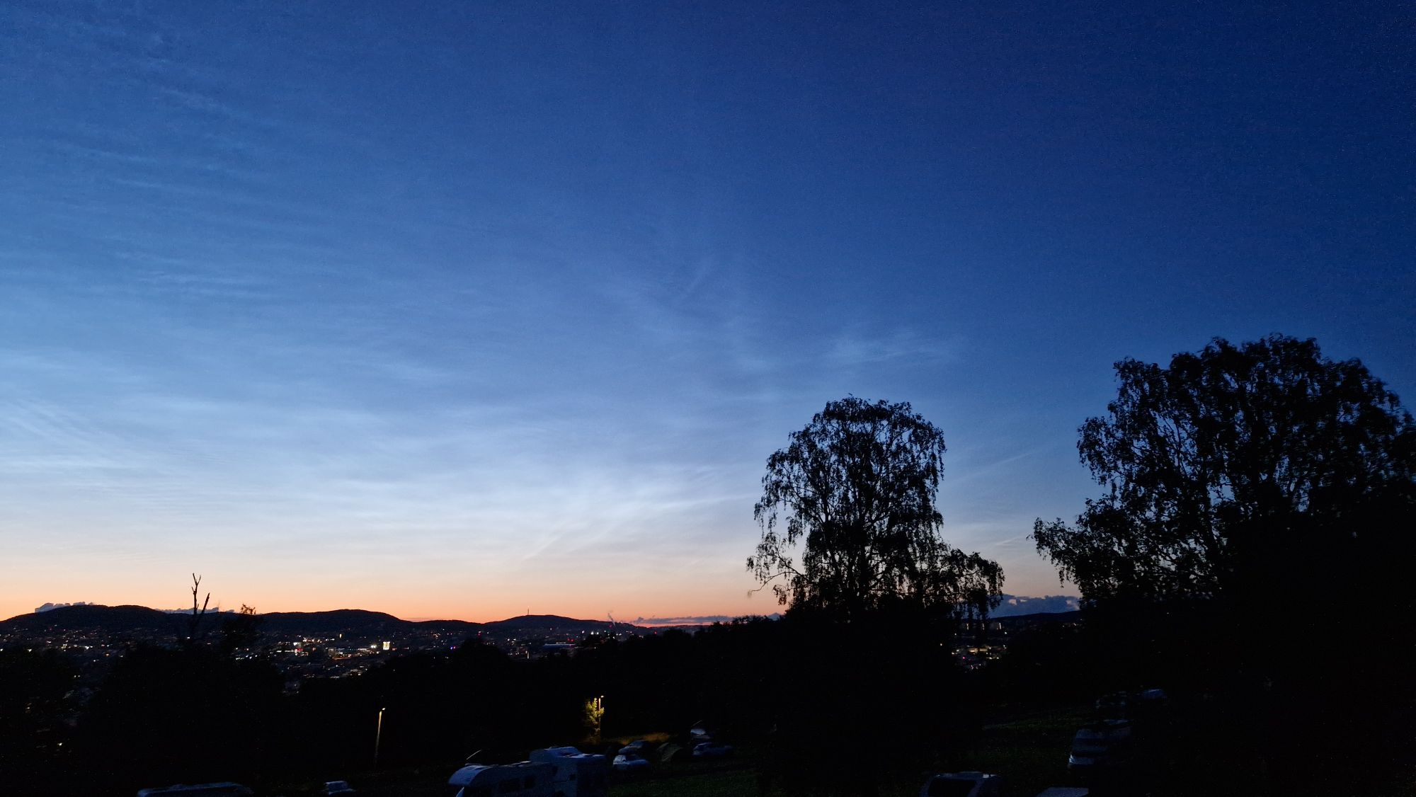
I decided to stay at Top Camp in Ekeberg. The price tag was high for a cyclist with tent: I paid 600 NOK for one night stay (approx. 50 EUR) which is almost double the price from Swedish camps. The quality of the camp site service house was disappointing: jammed toilet doors, clogged drain, prepaid card charging machine out of service. I couldn’t charge up my batteries. However, the tent area was large and spacy and the views on the cityline from the hill were awesome. I would not camp there again except in an emergency case like this.
View from Ekeberg at Oslo Central. Very niceNoctilucent clouds during night time
I will stay tomorrow (Friday) in Oslo and do some sightseeing. I don’t like the traffic and high price tags. Staying there will deciminate my travel budget very quickly. Therefore, moving on by evening may be a possible conclusion of my short visit…
100.2 km, 7h57m, average speed 12.58 km/h, 42.91 km/h max.
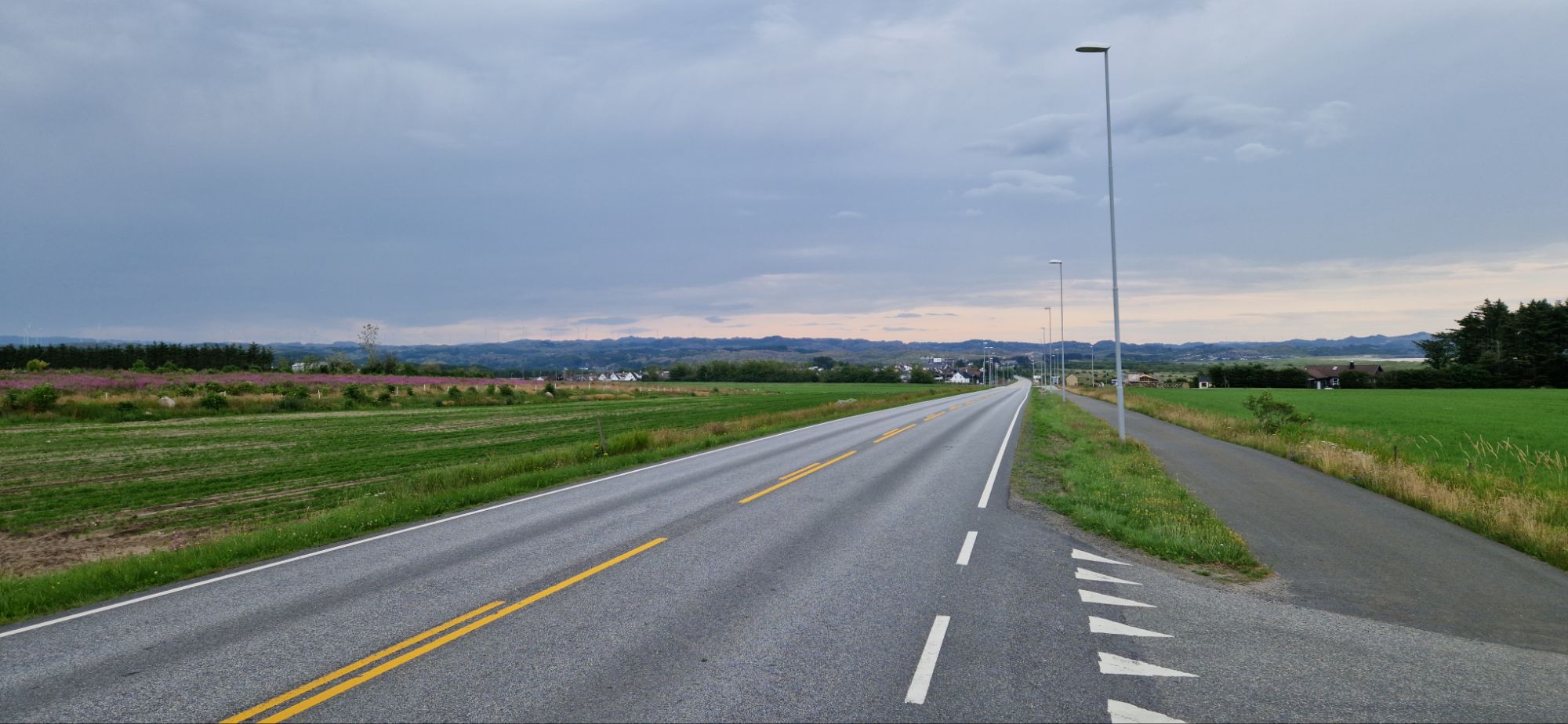
Wednesday, July 2nd. Woke up early in the morning to get some extra kilometers done. I was 10-15 km too short according to my plans. I was on the road quickly and the weather was OK for cycling: 18 °C overcast, no wind, a bit of rain clouds.
The cycle route was mostly on the regular road. The car drivers in Sweden and Norway were very nice so far and really friendly! I had no trouble and felt always safe on the roads. Thank you car drivers!
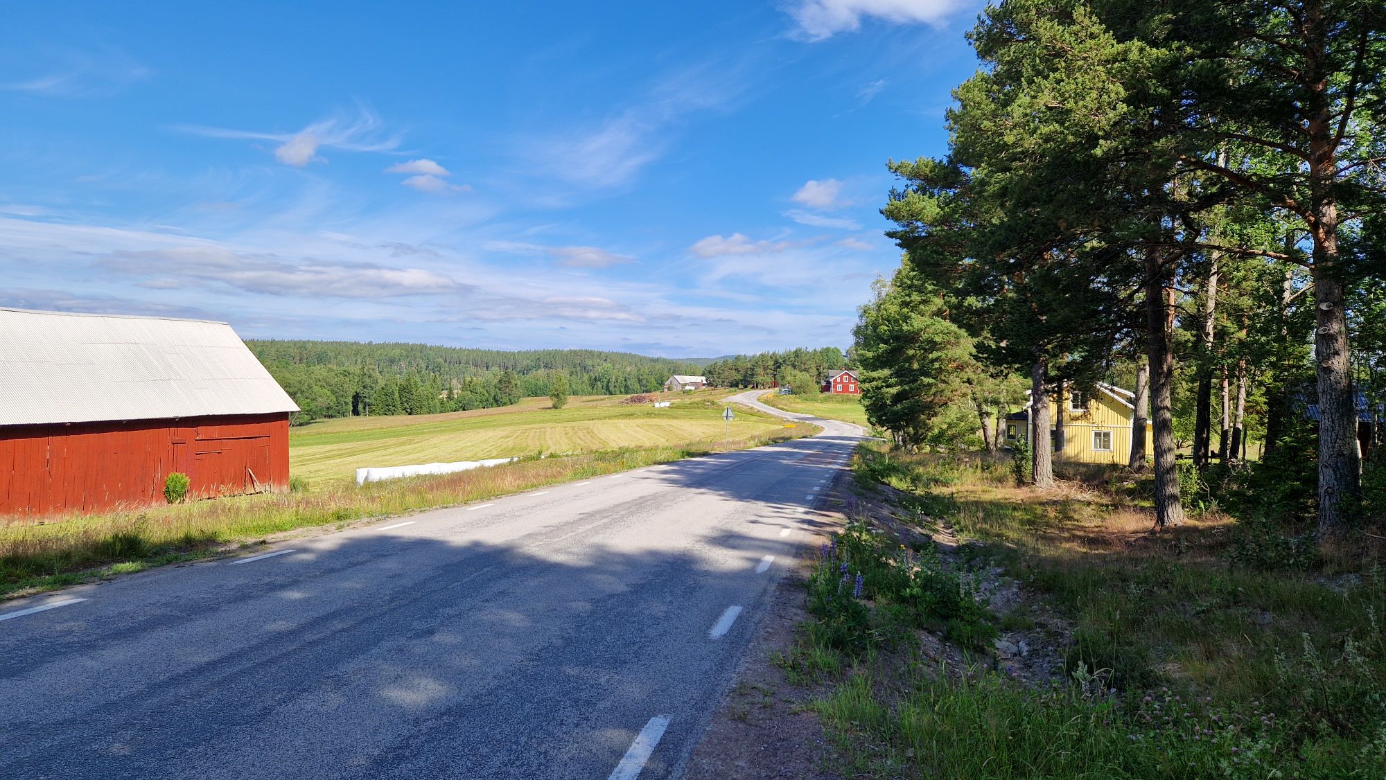
Typical road on this day, weather was fine
The route was challenging but I had to walk rarely due to steep hills. The walks were short, just few tens of meters to maybe 300 meters. I could maintain a good speed and progressed without large dificulties. I listened to music to mitigate the loud sounds of bypassing traffic and to get some variety.
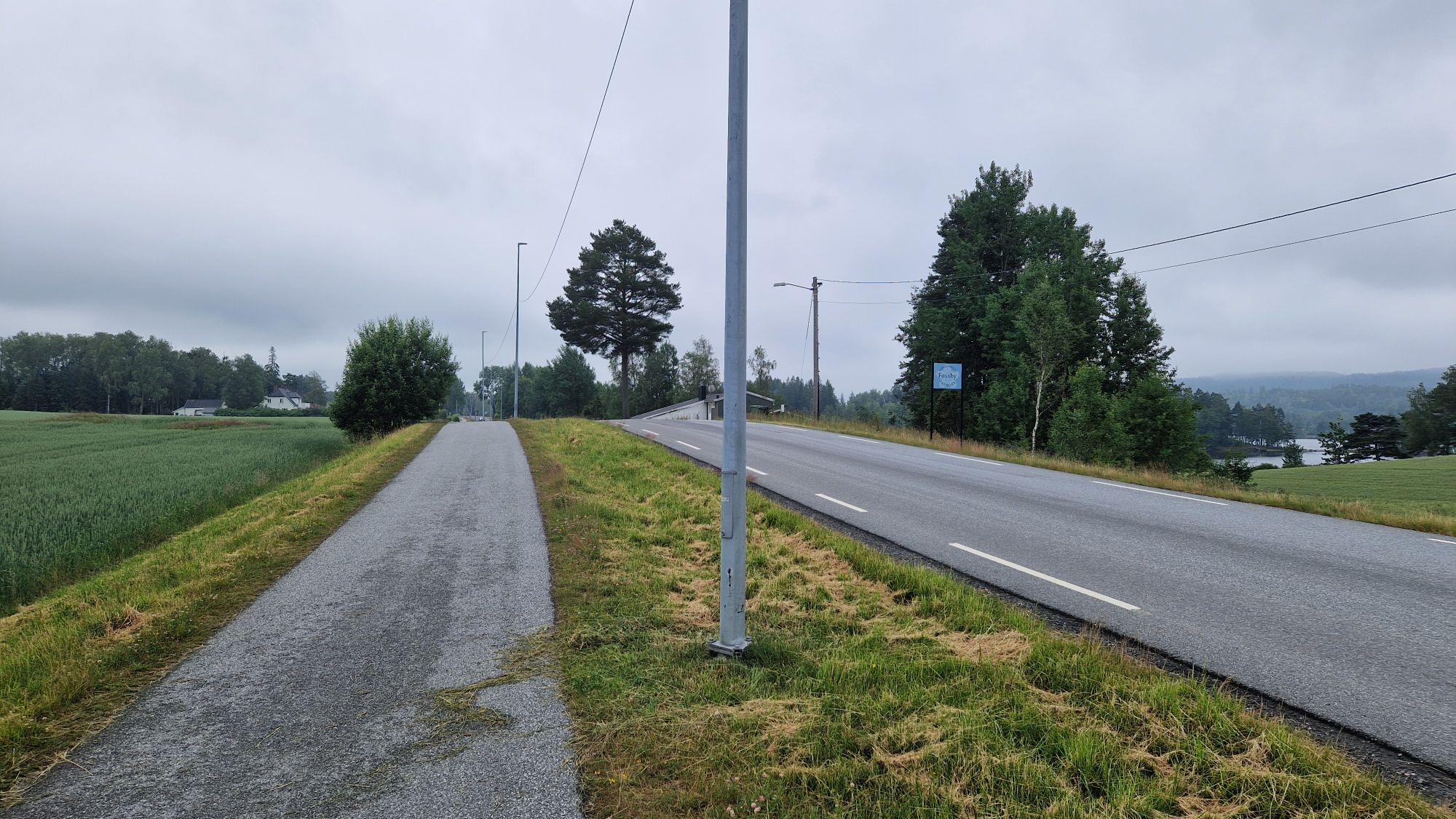
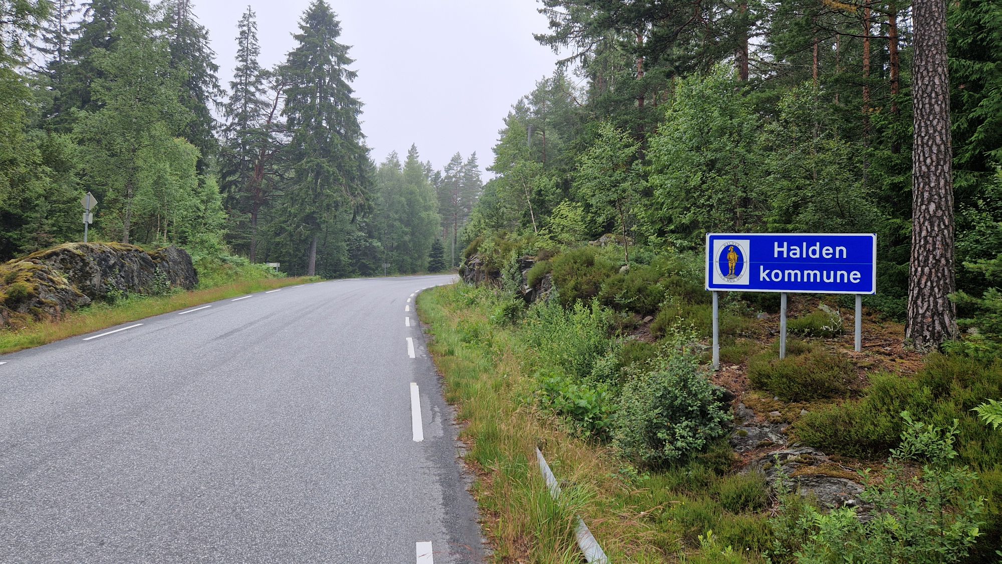
Entering Halden kommune
I reached Halden by noon and continued to Isebakke, just 3 km away from Swedish border. At this place, my old friend “Route 1” – The North Sea Cycling Route. From there, I continued cycling to Fredrikstad.
Sign pointing to Amundsen’s birthplaceAmundsen’s birthplace near FredrikstadRoald Amundsen statue in Fredrikstad
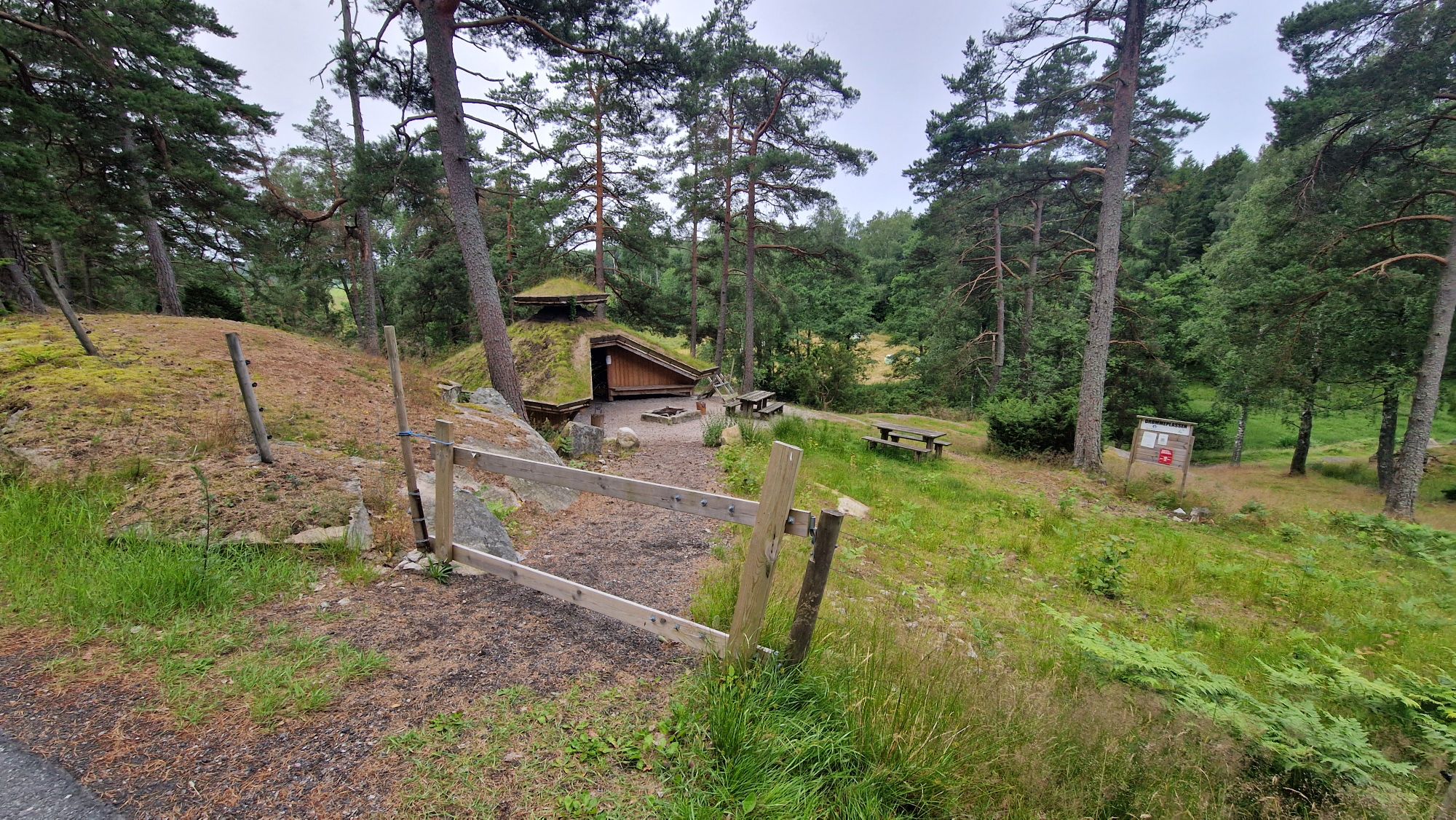
On my was to Fredrikstad I was close to the birthplace of Roald Amundsen, the famous Norwegian Explorer who reached the South Pole some 100 years ago. In Fredrikstad I took the ferry over the river and kept cycling 15 more kilometers. I found a very nice shelter near Elingård along the Route 1. Very unique and exciting day. Will hopefully reach Oslo tomorrow!
Shelter near Elingård
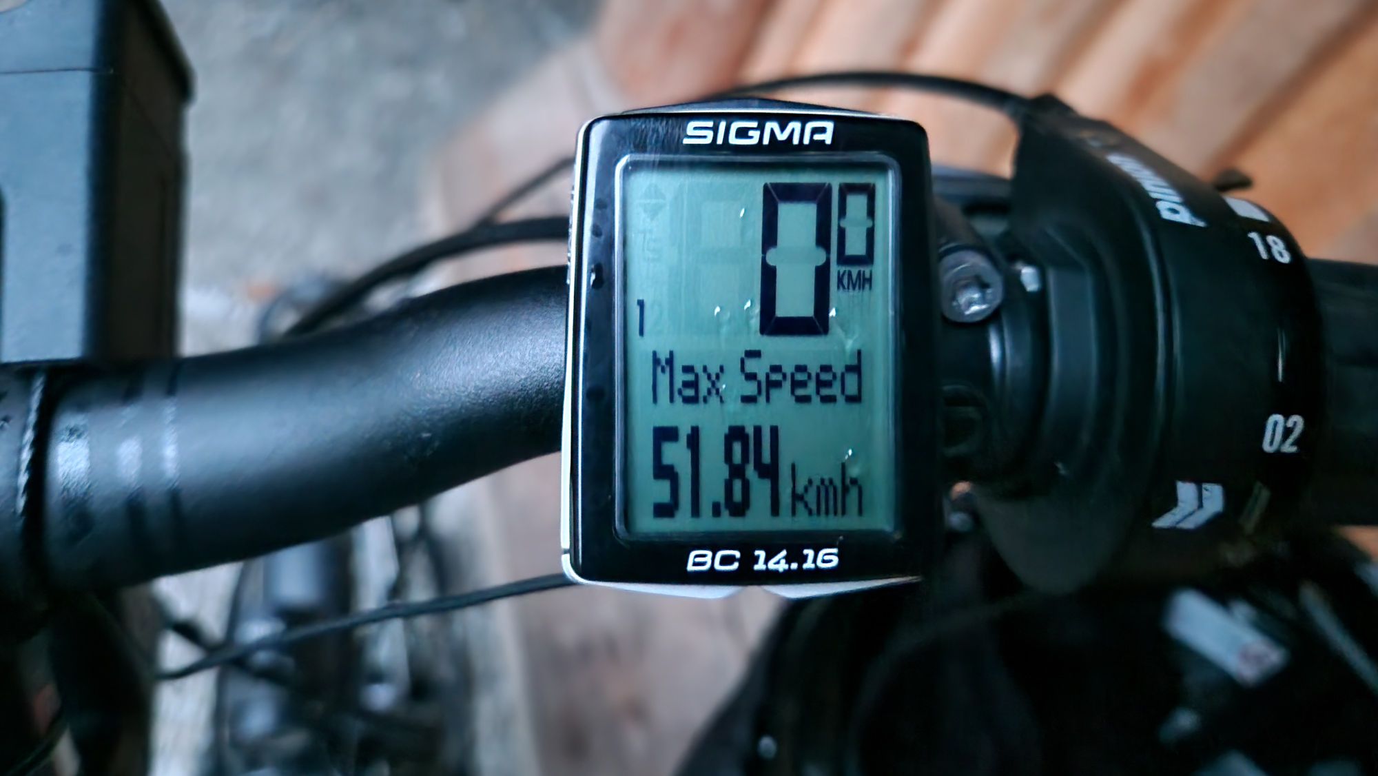
126.3 km, 9h10m, avg 13.78 km/h, max speed 51.84 km/h 😎
Tuesday, July 1st. After camping at Bengtsfors and charging up my batteries, the day started with sunshine and awesome weather forecast. I left the camp at 9:30am. The landscape changed to more forest and hills. My cycling route was mostly on the asphalt roads, which were great.
Nice weather and roads in Sweden
Cycling was challenging going uphill but I had to pull the bike just a couple of times. The gear range was sufficient for most hills. Racing downhill was the most fun part: fresh wind and high-speed feeling. This “up and down” repeated for the next 70 km or so until 11 km prior to Töcksfors.
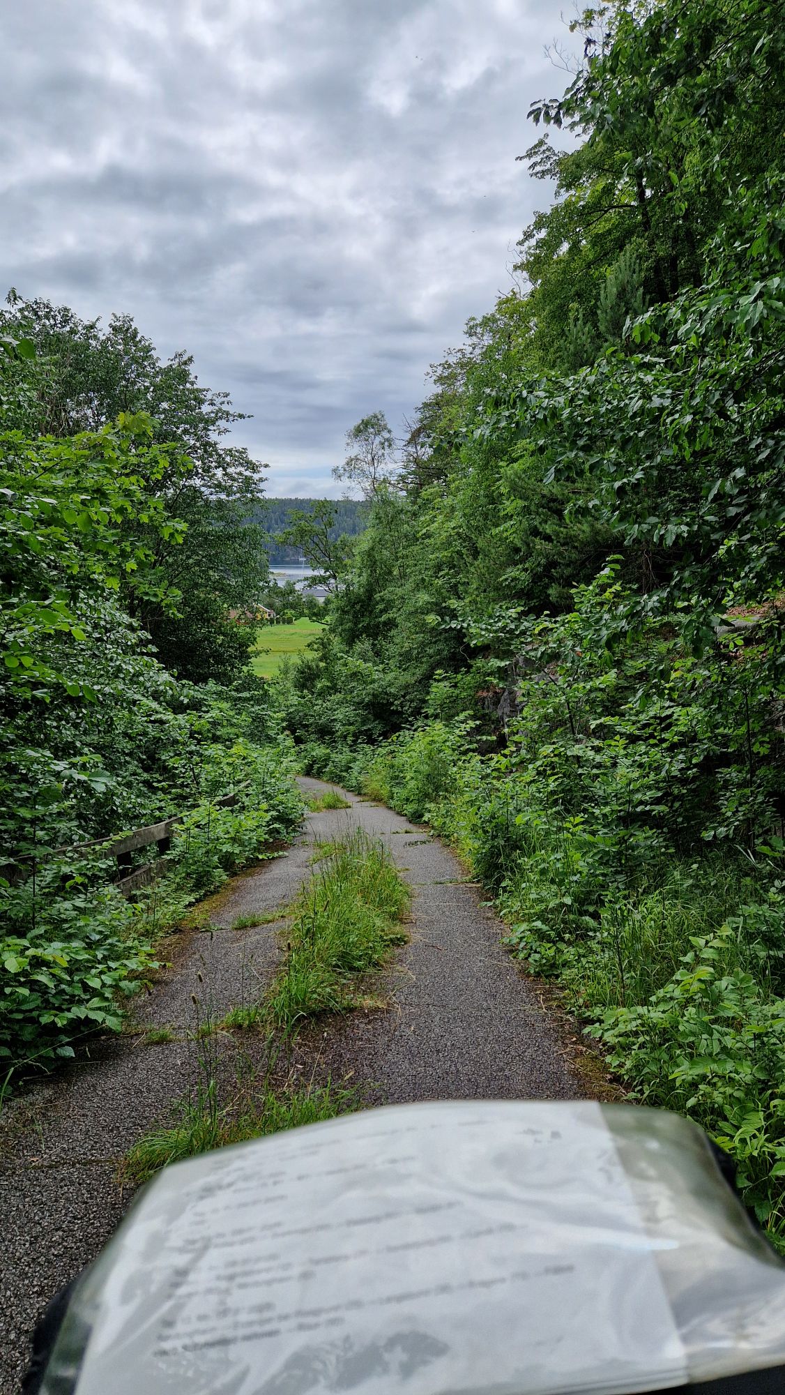
I kept following the Route 4 but the terrain changed suddenly to gravel/forest walk paths and steep terrain. The roads were rather made for mountain bikers than for regular travel bikes. I had to push my bike a lot and the mosquitoes started to bite me 😅
Walking this way instead of cycling
At some point and struggling ~1.5 hours, I reached Töcksfors. The morale was low so I had to eat something. I shopped some food before moving on to the border, which was only few kilometers away.
Gravel road near the border, me pushing my bike
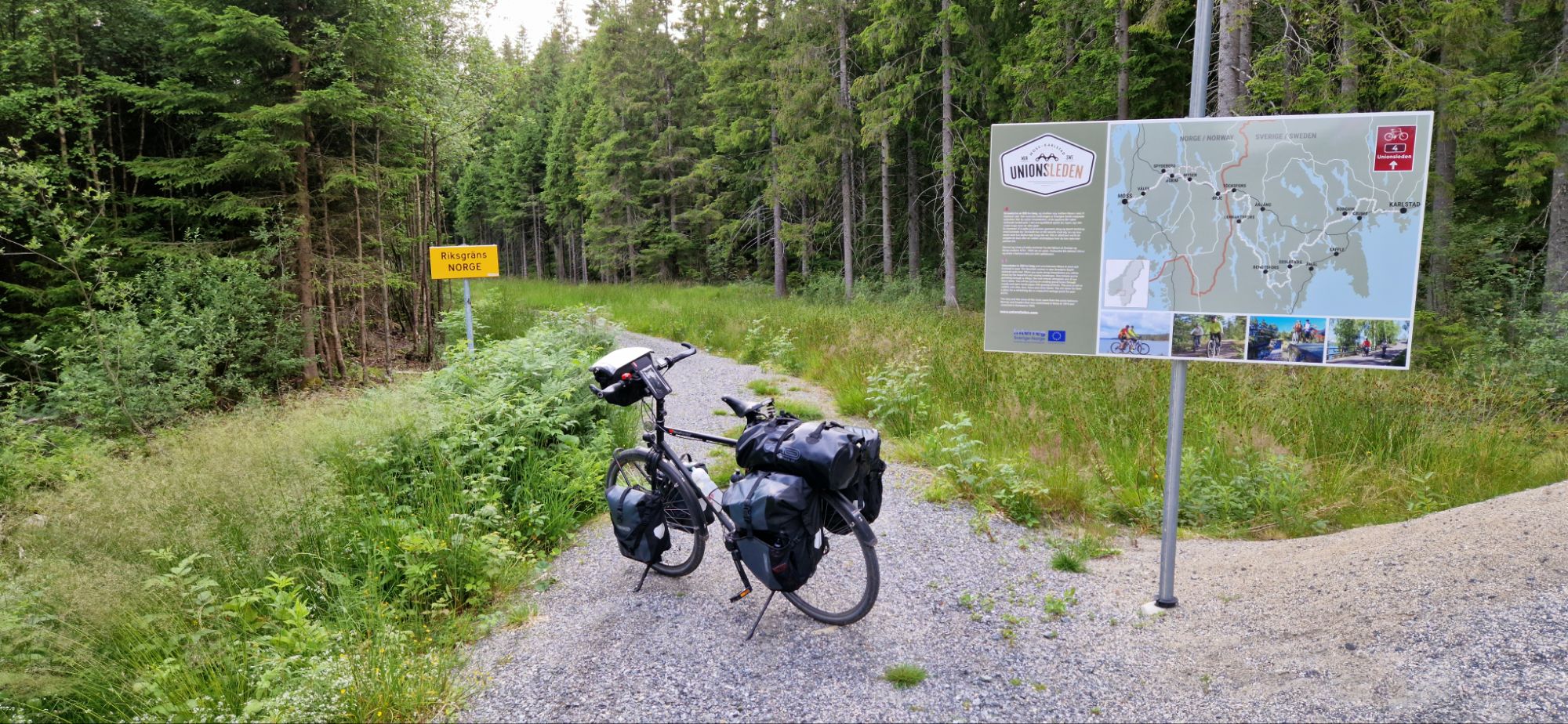
Everything went well until some 2 km prior to the border. The route changed from regular road to the well-known steep forest gravel thingy. So I had to literally push my bike and hike to the border.
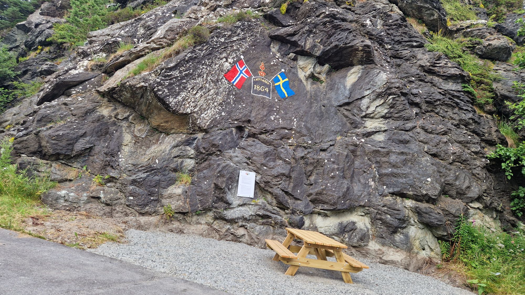
At this point, it was just annoying. Will I ever be able to ride my bike again? After 45 minutes of pushing uphill, I finally reached the Swedish/Nirwegian border. It was very rewarding and I was proud of achieving this.
Finally there! Swedish / Norwegian border
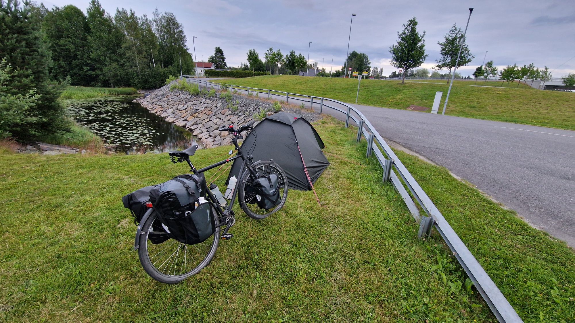
After walking a bit out of the forest and returning back to the regular roads, I cycled downhill to the next place called Ørje. I found a small camping spot at a local parking lot/rest area with toilets and set up my tent. There was another guy from France who also set up his tent. We talked a bit and got ready to get some sleep. The french guy told me he was hich-hiking from France to anywhere he wants and has already been in Vietnam… I was mind-blown by his story, bonne voyage!
“Emergency camping” in Ørje 😅
99.8 km, 8h19m, average speed 11.98 km/h, 51.7 km/h max.